2017
Color centers in nanodiamond. — Among the numerous optically active defects (color centers), studied in nanosized diamond (ND), the silicon-vacancy (SiV) center is a promising candidate for utilization in different fields like quantum computing and cryptography, nanoscopy, medicine or cell biology. Most applications are based on the intensive and narrow zero-phonon emission line (ZPL) of the mentioned color center, which can be detected in near infrared wavelength region, around 1.68 eV (738 nm). However, the asymmetric lineshape of the SiV ZPL may restrict the spectral parameters important for different applications and prohibit the determination of the real ZPL characteristics by traditional spectroscopic techniques.
Micro-photoluminescence measurements performed on a high number of CVD nanodiamond films containing SiV centers showed that the undesirable asymmetric tail on the low-energy side of the ZPL is related to another optically active defect (so-called GR1 center) being present in the nanodiamond structures as well. Regions with relatively high GR1 content and with well-distinguishable zero-phonon lines related to different optically active defect structures can be localized by mapping of the ND film with an appropriate excitation wavelength (Fig. 1).
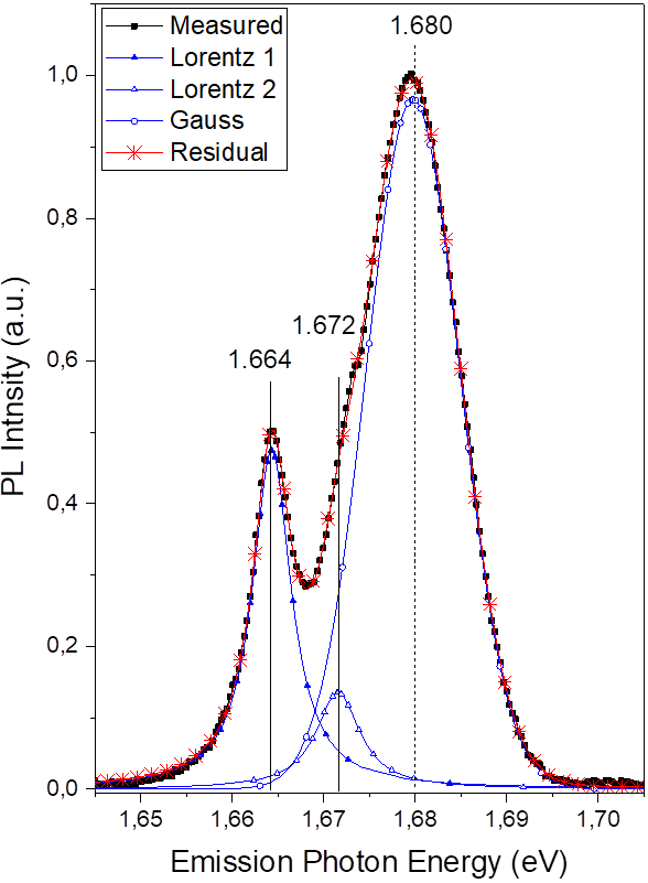
Figure 1. Fine-structured emission spectrum of CVD nanodiamond film around the SiV center ZPL region excited by 635 nm and recorded at room temperature. The deconvoluted peaks correspond to SiV center ZPL (1.680 eV) and the double ZPL of the GR1 defect (1.664 eV and the weak shoulder at 1.672 eV).
Preparation of new tetragonal silicon polymorphs by ultrashort laser pulses. — Tetragonal polymorphs of silicon were created successfully by irradiation of microcrystalline silicon powder with femtosecond laser pulses (800 nm center wavelength with 1 kHz repetition rate and 42 fs pulse duration) in air at room temperature. Surface enhanced Raman spectroscopy and, in collaboration with the Research Institute for Materials Science, Centre for Energy Research, HAS and the Research Centre for Natural Sciences, HAS, transmission electron microscopy (TEM) measurements were carried out to prove the presence of bt8 (Fig. 2) and t32* (Fig. 3) Si phases.
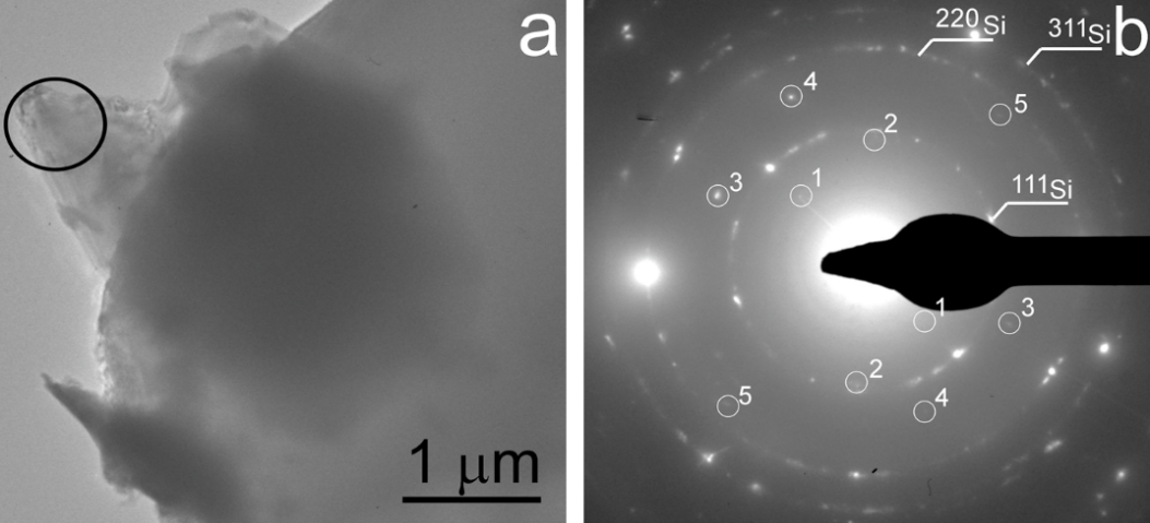
Figure 2. TEM image of bt8 Si polymorph. In addition to ordinary cubic Si, weak extra reflections occur with the following d spacings: 4.70 (1), 3.37 (2), 2.60 (3), 2.38 (4), 2.10 (5) Å. These extra reflections are consistent with {101} (1), {200} (2), {211} (3), {220} (4) and {301} (5) reflections of bt8 Si.
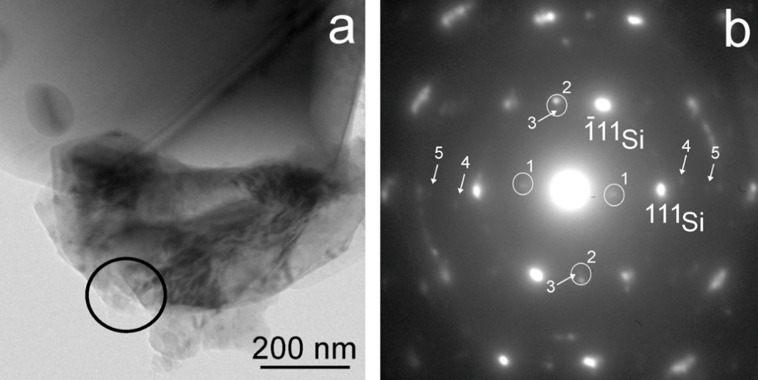
Figure 3. TEM image of t32* Si polymorph. In addition to ordinary cubic Si, there are two sets of strong reflections with 6.60 (1) and 3.20 (2) Å. These strong reflections and their measured angles are consistent with {110} and {0-12} of t32* Si grain. The additional weak reflections with 3.63 (3), 2.65 (4), 2.16 (5) Å can be interpreted with {211}, {311} and {013} of t32* Si.