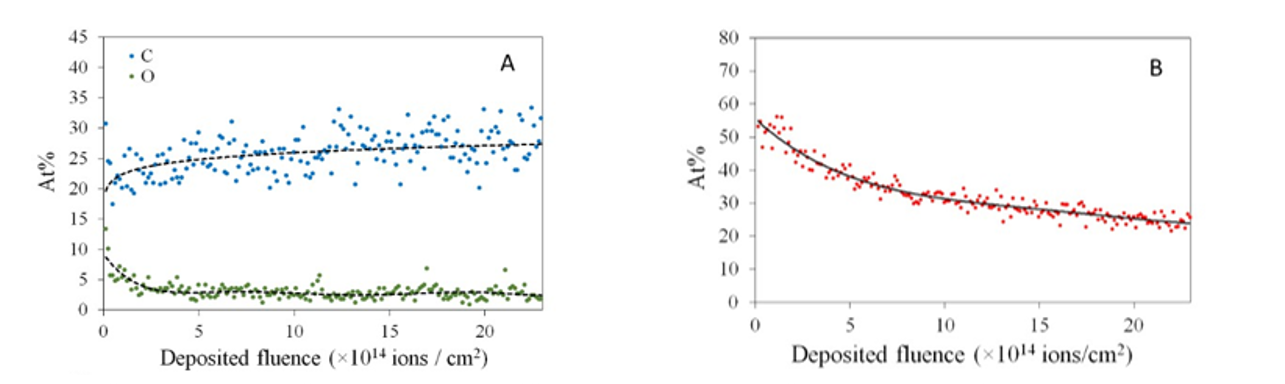
MTA Kiváló Kutatóhely
Hamburget Menu MTA.hu
  • MTA.hu főoldal
  • MTA tudományos hírek
  • MTA pályázatok
  • English
  • Hungarian
Címlap
HUN-REN Wigner Fizikai Kutatóközpont
ELKH ELKH

Main navigation

  • Rólunk
    • Vezetőség és Titkárok
    • Történet
    • Misszió és Évkönyv
    • Kutatóintézeti stratégia
    • MTA Kiváló Kutatóhely
    • Büszkeségeink
    • Közérdekű adatok
    • Alumni
  • Hírek
    • Hírek
    • Intézeti hírek
    • Állások
    • Médiamegjelenések
  • Kutatás
    • Kutatócsoportok
    • Infrastruktúra
    • Laboratóriumok és nyitott kutatási infrastruktúrák
    • Mesterséges Intelligencia
    • Futó projektek
  • Oktatás
    • Egyetemi kurzusok
    • OTDK eredmények
    • Szakmai gyakorlat
    • Nyílt napok, diákműhelyek
    • Középiskolásoknak, tanároknak
    • PhD képzés
    • Wigner Kollokvium
  • Kommunikáció
    • Médiatár
    • Brosúrák
    • Letölthető logók
    • Sajtóközlemények
    • Ismeretterjesztés
    • Kutatók éjszakája
    • Könyvkiadás
    • Wigner Café
  • Intranet
  • Kapcsolat

Ionnyaláb-fizikai Kutatócsoport

2023 


Fabrication of picowell arrays on polymer surfaces with a 10.5 MeV N4+ ion microbeam. — Handling of picoliter-to-nanoliter-scale volumes and objects has increasing importance in life sciences. This is the volume scale of cell extractions and individual living cells. A method of generating a picoliter-scale device by direct writing of picowell arrays on a ZEONOR™ copolymer surface with high-energy medium-mass ion microbeam was devised. Arrays of various microstructures were written in the sample using a microbeam of 10.5 MeV N4+ ions at various implanted ion fluences. The best array was obtained by implantation of annuli of 10 and 11 µm of inner and outer diameters with a fluence of 7.8·1012 ions/cm2. 

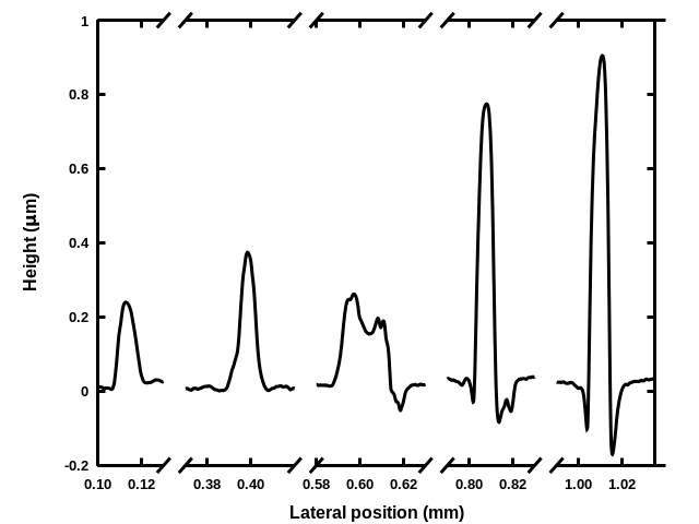
An array of 9 x 9 picowells, in the form of chalice-like structures, was obtained and tested. The implanted surface structures were studied by optical and atomic force microscopy (AFM). The average volume of the picowells was 820 femtoliter (fl), ideal to host a single living cell. AFM image of a picowell is shown in Figure 1.

ion


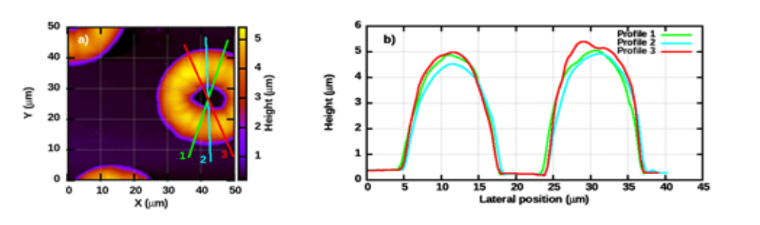
 Figure 1.  Height-contrast AFM image (A) of part of array J, and topographical height profiles of a picowell (B) in it. Sections of the picowell where profiles were extracted are indicated on the left panel.  


AFM microhardness measurements showed that the implanted toroidal wall of the picowell had the same hardness as the unimplanted parts of the sample. Applicability of the ion microbeam written picowell array in biomedical single-cell assays was demonstrated by placing individual cancer cells with the cell-cycle reporter fluorescent construct in some of the wells, and detecting their fluorescence signal. An example is presented in Figure 2, where microfluorescence from a HeLa Fucci cell placed in a picowell can be seen.
By changing the parameters of the fabrication, such as ion species, energy, fluence and ion microbeam size, reducing picowell volume down to about 100 fl and increasing the volume up to about 50 pl appear feasible. Thus direct writing of such structures using medium-to-high-energy ion microbeams can compete with direct writing by laser beam. A clear advantage of ion microbeam writing over laser beam writing is the better controllability in depth, allowing for fabrication of three-dimensional structures.

ion


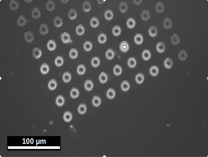
Figure 2.   A Fucci cell emitting strong fluorescent signal is seen in the targeted well. A 43HE DSRED filter was used.


Moreover, the recent introduction of ion nanobeam facilities with typical lateral beam sizes in the 200 - 400 nm range further improve lateral resolution of the ion beam irradiation technique. Although ion beam accelerators are normally not easily accessible, the proposed method has some clear advantages. First, it is a one-step fabrication. Second, it is a fast method: fabrication of an array can take typically tens of seconds and may take a maximum of a couple of minutes. The method permits a very quick and flexible design of the picowells. Third, besides the polymer used in these experiments, other materials, e.g. glasses can also be used, although higher fluences (and hence longer irradiation times) may be necessary. Finally, the fabricated surface structures can be also applied as templates for PDMS casting to obtain a negative replica. When a positive replica is needed, the PDMS stamps could be used for UV replication, obtaining by this way the exact copy of the fabricated structures.

Plastic deformation of microsamples. — Understanding how irradiation affects the microstructure and mechanical properties of various components is extremely important for nuclear applications. Investigations of bulk samples are hindered by the facts that neutron irradiation requires long exposure times and leads to the activation of the sample. For this reason ion irradiation is often used as an alternative since it was shown that the resulting defect structure is comparable to that caused by a neutron flux. However, the limited penetration depth of ions and the resulting inhomogeneity of the defect structure poses a significant challenge for the application of traditional tools of mechanical testing. Therefore, micromechanical approaches (such as nanoindentation or micropillar compression) have recently been used that exploit the fact that ion induced radiation damage can still be nearly homogeneous at microscopic scales.
Plastic deformation of microsamples is characterised by large intermittent strain bursts caused by dislocation avalanches. Here in collaboration with Department of Materials Physics, Eötvös Loránd University we investigate how ion irradiation affects this phenomenon during single slip single crystal plasticity [2]. For this purpose, in situ compression of Zn micropillars oriented for basal slip was carried out in a scanning electron microscope (SEM). The unique experimental setup also allowed the concurrent recording of the acoustic emission (AE) signals emitted from the sample during deformation. The results are summarized in Figure 3. 
 

ion


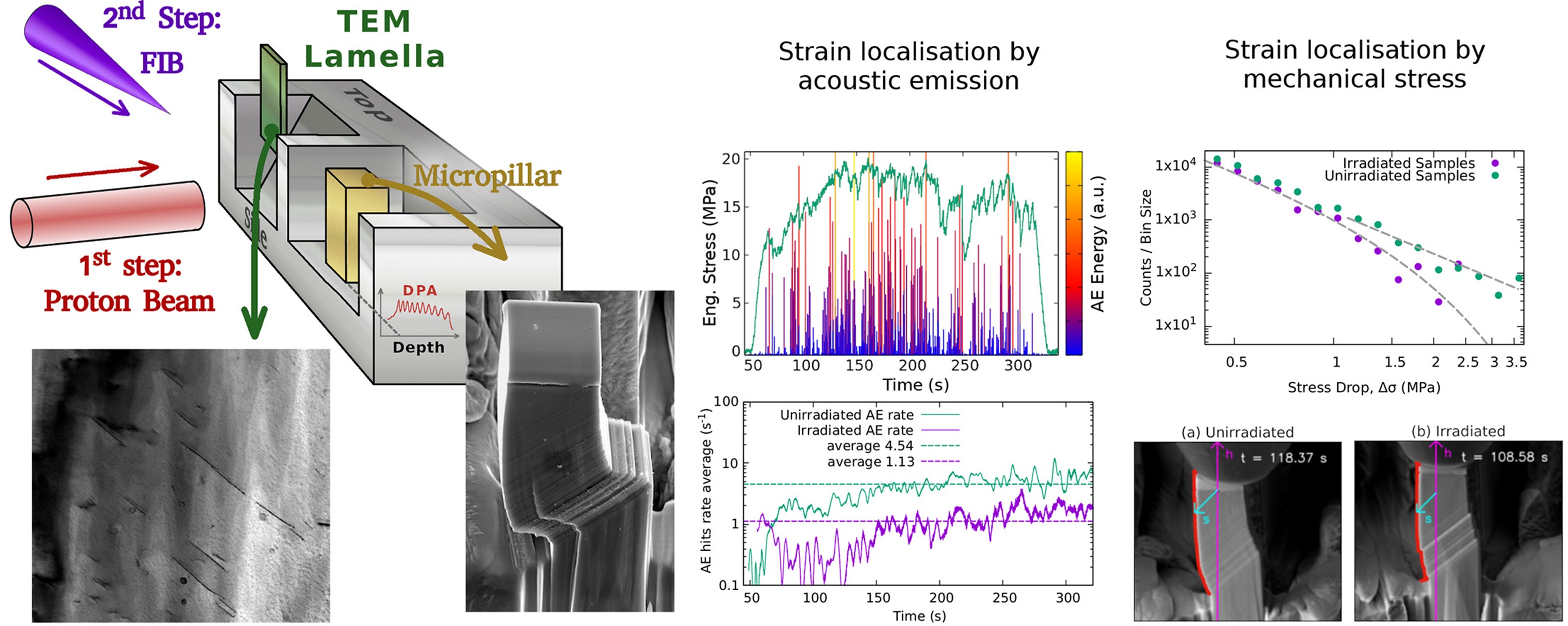
Figure 3. Schematic draw of the geometrical arrangement of the experiment, TEM image from an irradiated area showing the cross sections of irradiation-induced dislocation loops. Compression experiments were carried out on pristine and irradiated micropillars, SEM images show various micropillars. Acoustic emission was recorded concurrently during deformation. Strain was localized by acoustic emission and mechanical stress both for unirradiated and irradiated samples.


Irradiation introduced a homogeneous distribution of basal dislocation loops that lead to hardening of the sample as well as strain softening due to dislocation channeling at larger strains. Under the loading conditions imposed, the intensity of strain bursts was found to decrease during channeling. The concurrently recorded AE events were correlated with the strain bursts and their analysis provided additional information of the details of collective dislocation dynamics. It was found that the rate of AE events decreased significantly upon irradiation, however, other statistical properties did not change. This was attributed to the appearance of new type of dislocation avalanches which is dominated by short-range dislocation-obstacle interactions that cannot be detected by AE sensors.


References:
[1] Bányász I., Rajta I., Havránek V., Mackova A., Laki A. J., Kellermayer M. S. Z., Szittner Z., Kurunczi S., Novák Sz., Székács I., Horváth R., Fried M., Nagy G. U. L. Design, fabrication, and characterization of picowell arrays on cyclic olefin copolymer surfaces generated with a 10.5 MeV N4+ ion microbeam APPLIED PHYSICS LETTERS 123 : 5 Paper: 053701 , 6 p. (2023). DOI: 10.1063/5.0155681
[2] Ugi D., Péterffy G., Lipcsei S., Fogarassy Z., Szilágyi E., Groma I., Ispánovity P.D.: Irradiation-induced strain localization and strain burst suppression investigated by microcompression and concurrent acoustic emission experiments. MATERIALS CHARACTERIZATION 199 Paper: 112780, 11 p. (2023). DOI: 10.1016/j.matchar.2023.112780

2022

Various effects of ion implantation. —Spectroscopic ellipsometry (SE) is one of the most sensitive methods to use in the characterization of thin films, multi-layer structures as well as the change of crystallinity in semiconductors. To observe the dynamics of structural damage accumulation during ion-implantation, in collaboration with the Centre for Energy Research a real-time SE was developed in the chamber of Heavy Ion Cascade Implanter, as shown in figure 1. The real-time data also enable a more detailed insight into the dynamics of processes. Quantitative data such as the size of tracks created by the implanted ions, the volume fraction of phases, and the time intervals of quasi-periodic oscillations that can be observed in the three-dimensional reorganization process of the material structure.

ion1

Figure 1. For real-time SE measurements a Woollam M-88 spectroscopic ellipsometer with a rotating analyzer was mounted on a high vacuum chamber of the Heavy Ion Cascade Implanter. The vacuum chamber is equipped with high-quality entrance and exit windows to minimize the deviation in the polarization state of the measuring light caused by birefringence. The angle of incidence is fixed at 75°. The spectral range from 367 to 746 nm can be measured in 72 spectral points in every 3 seconds, simultaneously. The alignment of the sample can be realized by a 4-axis precision goniometer to maximize the reflected intensity, followed by an offset calibration. The sample holder includes a Faraday cup that reduces the typical value of uncertainty of the ion current measurement from 5-10% to 1%.

The aim of the first experiment [1] is to give a description about dynamics of the complex process of amorphization and void formation in the technologically important case of shallow implantation profiles formed in Ge. For this, the single crystalline Ge sample was implanted by heavy Sb ions, and the time evolution of disorder and morphology changes induced by ion bombardment in c-Ge were followed by real-time SE measurements. Complete spectra were recorded in the visible-near ultraviolet wavelength range in each 3 s during the implantation of 200-keV Sb ions with a total fluence up to 1016 cm−2 and an ion flux of 2.1×1012 cm-2s-1.

In our previous work [2], the complex dielectric function of i-a-Ge was determined by SE in a broad wavelength range (from 210 to 1690 nm). This result was used as a basic component during the evaluation of the present real-time measurements. Each SE spectrum, collected during Sb implantation, was evaluated according to the four regions. Regions I, II, III and IV refer to the “unimplanted”, “damage accumulation”, “rapid void formation” and “slow change of damage and voids” cases, respectively. This covers approximately 90 minutes of measurement with 3 s steps, i.e., almost 2000 individually fitted spectra. The fluence of 1x10¹⁴ is just sufficient to amorphize the first 50 nm and the second 50 nm is only partially amorphized of the Ge surface layer. During the next implantation (up to 1x10¹⁵) the second 50 nm is amorphized gradually, visible as an a-Ge layer with gradually increasing thickness.

To follow the evolution of the different parameters, such heavily and slightly modified thicknesses, volumetric ratios of c-Ge, i-a-Ge and void content we fitted the parameters of a complex optical model as shown in Figure 2. By comparing this results with scanning electron microscopy and ion beam modelling, the optical properties of amorphized and porous nanostructures could be identified that obtained by Sb ion implantation of c-Ge.

ion2

Figure 2. Evolution of the SE determined modified layer thickness and sublayer thicknesses (areas separated by a solid red line). The composition of the sublayers is denoted by the volume fraction of the components of i-a-Ge (dark grey areas denoted by ‘a’), void (light grey areas denoted by ‘v’) and c-Ge (light blue area denoted by ‘c’) as a function of time. The ratio of the areas covered by the individual components on both sides of the solid red line is proportional to their volume fractions. The fitted parameters were the thicknesses of the sublayers (uncertainty of a few nm) and the volume fractions (uncertainty of a few %) of i-a-Ge and void. The regions of damage formation I-IV are also marked by vertical lines. The white area is the single-crystalline substrate.

2021

Various effects of ion implantation. — Optical channel waveguides have been designed and fabricated in a large number of crystalline and glass samples via ion microbeam irradiation. Notable target materials were sillenite and eulytine type BGO, LiNbO3, KTP and RTP optical crystals, IOG and Pyrex glasses and Er:Te-W glass. Nitrogen, carbon and oxygen ions in the 10 – 15 MeV energy range were used in the irradiations. Structural tests have recently been supplemented by high-resolution surface mapping using a Sensofar contactless device and micro Raman spectrometry [1, 2]. Step wise thermal annealing of the irradiated channel waveguides proved to be an excellent means to reduce propagation losses by over a decade.

IF1

Figure 1. Electronic (dots) and nuclear (triangles) energy loss vs. depth in an Er: tungsten-tellurite glass irradiated with 11 MeV C4+ ions. Note that nuclear energy loss was multiplied by 10 for better visibility.

IF2

Figure 2. Surface profile of five channel waveguides as implanted in an Er:-Te-W glass with C3+ microbeam of E= 11 MeV. Irradiated fluences from left to right: 1·1014, 2.5·1014, 5·1014, 1·1015 and 1.5·1015 ion/cm2.


The use of swift heavy ions in the ion beam fabrication of integrated optical elements reduced the necessary fluence and hence irradiation time between one and three decades, since for such energetic ions the predominant interaction with the target is electronic (see Figure 1.)
Ion beam written channel waveguides were also studied by profilometry (Bruker Dektak XT, tip radius: 5 μm) to check for possible surface relief structures. Indeed, it was found that the irradiation by focused carbon ions produced considerable swelling of the glass sample. Surface profiles of five as implanted channel waveguides are shown in Figure 2.

To obtain information on the structural changes produced by the ion microbeam irradiation in the channel waveguides, micro Raman spectroscopy was performed with a Renishaw 1000 micro Raman spectrometer. Full width at half maximum (FWHM) of a 922.3 cm-1 Raman line across two channel waveguides, irradiated with a carbon microbeam of E= 11 MeV at fluences of 4.16·1015 ion/cm2 (as implanted) and 4.6·1015 ion/cm2 (annealed) are presented in Figure 3.

IF3

Figure 3. Full width at half maximum of the 922.3 cm-1 Raman line across an as implanted (blue line) channel waveguide, irradiated with a carbon microbeam of E= 11 MeV at a fluence of 4.16·1015 ion/cm2, and a thermally annealed (red line) channel waveguide, irradiated with a carbon microbeam of E= 11 MeV at a fluence of 4.6·1015 ion/cm2.

Guided wave propagation in each channel waveguide was tested at λ=1540 nm and insertion losses were measured at 1400 nm, outside the absorption band of Er3+. Measured as-implanted, net propagation losses of all the channel waveguides were in the range 14–20 dB/cm. The channel waveguide irradiated with a fluence of 4.6·1014 ion/cm2 presented the lowest propagation loss, 14 dB/cm. A stepwise annealing up to 300 Cº was applied to the sample to reduce propagation losses. Results are presented in Figure 4.

IF4

Figure 4. Losses vs. temperature of the 30-minute annealing steps measured at 1400 nm. F = 4.6·1014 ion/cm2.


References:
[1] I. Bányász et al., Fabrication of low-loss optical channel waveguides for the telecom C band in rare-earth doped optical glass using microbeam of 11 MeV carbon ions, Optical Materials: X,  Volume 4, December 2019, 100035 (2019). https://doi.org/10.1016/j.omx.2019.100035

[2] I. Bányász et al., Ion Beam Implanted Channel Waveguides in an Er-doped Tellurite Glass, in: Proceedings of the 4th International Conference on Optics, Photonics and Lasers (OPAL' 2021), 13-15 October 2021, Corfu, Greece, pp. 80-83, S.Y. Yurish, Editor, IFSA Publishing, ISBN: 978-84-09-34187-0, BN-20211008-XX, BIC: TTB

2020

Various effects of ion implantation. — In collaboration with the Functional Nanostructures Research Group of Wigner RCP, reversible control of magnetism in FeRh thin films has been demonstrated [1]. Manipulation of magnetic and structural properties of FeRh is possible by ion irradiation and annealing. A thin film [nFe51Rh49(63 Å)/57Fe51Rh49(46 Å)]10 was deposited by molecular beam epitaxy on MgO(001) substrate at 200 °C. The film had an approximate composition Fe51Rh49 as determined by Rutherford backscattering spectrometry (RBS) and conversion-electron Mössbauer spectroscopy (CEMS). The deposited film contained primarily the paramagnetic A1 phase with a minute contribution from the magnetic B2 phase. The as-deposited state was fully converted to the magnetic B2 phase by annealing at 300 °C for 60 min. Subsequent irradiation by 120 keV Ne+ ions with a fluence of 1 × 10¹⁶ at/cm2 turned the thin film completely to the paramagnetic A1 phase. Repeated annealing at 300 °C for 60 min resulted in 100% magnetic B2 phase, a process that seemed to be suitable for being repeated reversibly several times. These results open the way to fabricating nearly equiatomic FeRh thin films of designed lateral magnetic/non-magnetic structure for future applications in spintronic devices. Possible approaches may be both lithographic techniques and heating by focused laser-beams.

ion beam 1

Figure 1. a) The element/isotope concentration depth profile from the concurrent evaluation of RBS and neutron reflectometry data. b) Contribution of the ferromagnetic B2 and paramagnetic A1 FeRh phases to the CEMS spectrum.

In collaboration with the Centre for Energy Research, complex dielectric function of ion-implanted amorphous germanium was determined by spectroscopic ellipsometry [2]. Accurate reference dielectric functions play an important role in the research and development of optical materials. Libraries of such data are required in many applications in which amorphous semiconductors are gaining increasing interest, such as in integrated optics, optoelectronics or photovoltaics. The preparation of materials of high optical quality in a reproducible way is crucial in device fabrication. Amorphous Ge (a-Ge) was created in single-crystalline Ge by ion implantation. The optical properties were measured by multiple angle of incidence spectroscopic ellipsometry identifying the Cody–Lorentz dispersion model as the most suitable, that was capable of describing the dielectric function by a few parameters in the wavelength range from 210 to 1690 nm. The results of the optical measurements were consistent with the high material quality revealed by complementary RBS and cross-sectional electron microscopy measurements, including the agreement of the layer thickness within experimental uncertainty.

Advanced cultural heritage research. —Archaeological finds from a settlement of the early Urnfield culture dating from the Ha A1 period (13th/12th century BC) and located at Nagykanizsa–Bilkei-dűlő (County Zala) in Southern Transdanubia included a small mug decorated with a longish knob and three rounds, regularly spaced stamped motifs retaining the residue of a whitish substance (Fig. 1a). A larger amount of this substance survived in one of the stamped circles- In the preliminary report of the excavation it was suggested that this substance perhaps represented the remains of a glass inlay  [L. Horváth: Késő bronzkori település feltárása Nagykanizsán. Excavation of a Late Bronze Age settlement at Nagykanizsa. Archaeological Reports in Hungary (1997) MNM Budapest, 2001, 37-43).].

At the request of an archeologist of the Pázmány Péter Catholic University, Piliscsaba, Hungary the composition of the remains were analysed by external beam PIXE (Particle Induced X-ray Emission) spectroscopy which revealed that the substance was not glass because it contained high amounts of copper (Cu) and tin (Sn) (Fig. 1b) Alloys of this type are generally referred to as white bronze in archaeological studies.  The objects with a high tin content represented a significant value, on the one hand they were used to make jewelry imitating silver, and on the other hand they could also be used as a raw material essential for bronze casting.

Ion_beam2

Figure 1. a) The tile mug in measuring position   b) External milli-beam PIXE spectra

2019

Various effects of ion implantation. — A novel method has been demonstrated in collaboration with Centre for Energy Research, to produce SiC patterns at room temperature, which is scalable up to wafer size. Two differently masked (LB film and lithographic grid) Si (20nm)/C (10nm)/Si(20nm)/C (10nm) /Si substrates have been irradiated by 120 keV, 3×10¹⁶ Xe+/cm2. Due to ion beam mixing a SiC rich layer formation on the non-covered parts of the sample can be observed, while the covered regions have not changed.

In collaboration with Atomki, Nuclear Physics Institute (Czech Republic), Institute of Applied Physics “Nello Carrara” (Italy) and University of Verona (Italy), a new method, i.e., direct writing with high-energy focused microbeam of medium-mass ions at low fluences, has been realized for the fabrication of optical channel waveguides. The lowest propagation loss in a Er3+ doped tungsten-tellurite glass waveguide, measured at a wavelength of 1400 nm after a 30 min thermal annealing at 150 °C, was 1.5 dB/cm. Due to the predominant electronic interaction, a fluence of 4.6·1014 ion/cm2, more than an order of magnitude lower than those applied in low-energy implantation, was sufficient for effective waveguide formation. The low losses of the fabricated waveguides open the use of this technique to test the fabrication of planar guided optical amplifiers and lasers in materials such as tellurite glasses where it can be difficult to use other techniques.

Radiation tolerance of organic materials has been investigated in collaboration with Atomki. Polymers have exact and known chemical structure, so they are ideal model materials to study ion beam irradiation induced chemical processes. Real-time Rutherford backscattering spectrometry and elastic recoil detection (RBS/ERDA), which was implemented to monitor the hydrogen loss caused by the He-irradiation used for the analysis itself, revealed that the hydrogen content decreased significantly. The formation of small molecule fragments and their escape from the sample was followed indirectly by RBS, simultaneously with the ERDA measurements. At lower fluences the oxygen content decreased as well. RBS/ERDA completed with infrared spectroscopy proved to be an excellent tool to study the changes of poly(methyl methacrylate) (PMMA) upon He+ irradiation, and thus to further our understanding of the complex chemical processes taking place (Fig. 1).

Advanced cultural heritage research. — Within the frame of EU IPERION CH project, non-destructive compositional analyses were performed on glass objects found in archaeological excavations from Dobroudja at the border of Black Sea. The findings were shards of late Roman glass (III-VI Centuries AD) and fragments of coloured Byzantine bracelets (X-XII Centuries AD).  The analyses were done by external milli-beam PIXE (Particle Induced X-ray Emission spectrometry) with 2.5 MeV protons at Wigner RCP and by PGAA (Prompt Gamma Activation Analysis) at the cold neutron beam of the Budapest Research Reactor (Centre for Energy Research).  PGAA analyses have shown that the Roman Imperial glasses are soda-lime-silica glasses using natron (a substance containing sodium salts from some lakes in Northern

ion-beam physics1


Figure 1. The oxygen and carbon (A) and hydrogen content (B) changes of the PMMA polymer caused by 1.6 MeV He+ ion irradiation, measured by real-time RBS/ERDA. Symbols: concentration of carbon, oxygen and hydrogen evaluated from 200 successively recorded spectra taken on the same spot of the sample with a dose of 0.02 µC. Lines: fitted exponential curves.

Egypt as flux. The detection of Sb by PIXE has indicated that to obtain the transparency of the primary glass Antimony oxide was used as decolourant. This result has also supported the Northern Egyptian origin of the primary glasses. All the coloured Byzantine fragments were made from soda-lime glass, proving that commerce with Egypt, the main source of natron was still active. In colouration yellow pigment based on Pb and Sn (as shown in Fig.2). White, green, blue and dark blue paintings contained Ca, Cu, Fe and Mn, respectively.

ion-beam physics2

Figure 2. Yellow pigment on a Byzantine bracelet: a combination of Pb and Sn dye.

2018

Charge accumulation — Insulator materials have scientific and technological importance in diverse areas such as thermo-isolating coatings for spacecraft, optoelectronics solar panels, and applications of polymers, etc. During the bombardment of insulator materials with energetic particles, i.e., during ion implantation or ion beam analysis, the samples are often emitting light and are sparking. 

Analysing insulator samples, due to charge accumulation on the beam spot a potential difference DU will be formed between the sample surface and the ground (e.g., sample holder), which is able to decelerate the incoming beam particles before they reach the sample and to accelerate the reaction products when they leave the sample surface. These deceleration and acceleration processes will modify the energy spectrum of the reaction products. In addition, due to the sparking, the potential difference DU is not stable during the experiments. The fluctuation dU will introduce new energy spread contributions to the conventional ones.

Despite all the efforts to eliminate the charge accumulation using thin cover layers, wrapping or masking the samples, applying relatively low beam currents or electron sources, sometimes the samples may be charged. Ion beam analysis spectrum evaluation code, DEPTH was extended by a module implementing a new model accounting for charging-up effects. The results are shown in Fig.1.

sziledit


Figure 1. Comparison of He-BS spectra taken on 30 nm BaTiO3 layer on MgO substrate. a) Using Pt cover layer, b) with and c) without electron source. Vertical arrows represent the surface positions of Pt, Ba and Ti according to the energy calibration. Lines for various simulation by DEPTH. In Fig. a) and b) no charge accumulation is occurred. In Fig. c, the sample is charged up to DU=38 kV, dU=22.5kV. Dashed lines represent the charge state of outgoing ions (0, 1 and 2). Solid line represents DEPTH simulation, when the energy dependent charge state distribution is substituted by the two most abundant charge states.

In Fig 1 2 MeV He-BS spectra taken on BaTiO3 thin layer on MgO substrate are shown. By covering partially the sample with 5 nm thick Pt layer (Fig. 1a) no charge accumulation occurred on the covered region. To eliminate the charge accumulation in the non-covered region, an electron source was used during the experiment (Fig. 1b) while spectra taken without using electron source are shown in Fig.
1c. Due to the energy dependence of the charge distributions, the charging-up spectrum cannot be interpreted by a simply linear combination of simulations calculated for charge states 0, 1 and 2. This is well visible in Fig. 1c. For the correct interpretation of the electrostatically charged up spectrum the energy dependent charge state distribution is substituted with the two most abundant charge states calculated from Zmean, gives a very good agreement with the experiment.

Advanced cultural heritage research. — Archaeological artefacts, blackish grey beads of unknown nature that come from a funerary feature used for the secondary deposition of cremated remains located in the centre of Perdigões (Évora, Portugal) dated from the third quarter of the 3rd millennium BC were studied. In the context of IPERION CH cooperation a wide range of non-destructive techniques were applied, external milli-beam particle induced X-ray emission spectroscopy (PIXE), prompt-gamma activation analysis (PGAA), and high-resolution time-of-flight diffractometer (ToF-ND). In some cases infrared spectroscopic (FTIR) and Scanning Electron Microscopy coupled with Energy Dispersive X-ray Spectrometry (SEM/EDX) measurements were also performed. The surface chemical composition obtained by PIXE and the bulk analysis by PGAA and ToF-ND indicate, that the most probable raw materials for the blackish grey beads manufacture were shells.

szile

The PIXE measurements were performed at the 5MV Van de Graaff accelerator of the Institute of Particle and Nuclear Physics, Wigner Research Centre for Physics, Hungarian Academy of Sciences.

2017

Various effects of ion implantation—Corrosion resistance of silicon carbide (SiC)-rich nanolayers produced by implantation and damage caused by radiofrequency sputtering of niobium oxide have been studied in collaboration with Institute of Technical Physics and Materials Science, Centre for Energy Research.

To produce SiC protective coatings C/Si/C/Si/C multilayer structures with different thicknesses on silicon substrates were irradiated by Ar+ and Xe+ ions at room temperature and at a fluence range of 0.5–3x10¹⁶ ion/cm2. The C, Si and SiC distributions formed by the effect of ion beam mixing were determined by Auger electron spectroscopy. In corrosion point of view the best SiC-rich layer was produced from multilayer with thicknesses of 10 nm C and 20 nm Si by implanting with 120 keV Xe with a fluence of 3x10¹⁶ Xe/cm2. As a result of the potentiodynamic experiments, the measured chemical corrosion resistance for this sample was orders of magnitude better than that of pure silicon.

To investigate the damage caused by radiofrequency sputtering, Nb2O5 layers were deposited to c-Si substrates in a gas mixture of O2 and Ar at a pressure of 0.3 Pa, at an oxygen flow of 6 ml/min and at various DC sputtering voltage selected from the range of 1.0–2.0 kV. During the rf-sputtering the energetic O+, Ar+ ions and neutral atoms may penetrate into the c-Si substrate to a depth of several nm causing displacement of host silicon atoms and consequently producing damaged regions.

In cross-sectional transmission electron microscopy image of a Nb2O5 sample with a deposition time of 100 s at 2.0-kV (not shown) a 2.9 nm thick amorphous Nb-oxide film, a 4.5 nm thick amorphous layer, which can be either amorphous SiO2 and/or amorphous Si, as well as single crystalline substrate can be observed. The partially damaged silicon layer was identified on the substrate both by Rutherford backscattering spectrometry combined with channelling (as shown in Figure 1) and by multiple angle of incidence spectroscopic ellipsometry.

f1

Figure 1. Channelled and random spectra taken on Nb2O5 film deposited by rf sputtering on single crystalline silicon substrate with a deposition time of 100 s at 2.0-kV. 

Advanced cultural heritage research. — External milli beam PIXE was applied to determine the composition of mineral pigments from ceramics objects excavated by Romanian archaeologists from archaeological sites of important commercial settlements on Danube at the border between Ottoman Empire (Dobroudja) and Romanian Principalities – Piua Petrii and Dinogetia-Garvan.. The mineral pigments used for Turkish Miletus (late XVth-XVIth centuries) and Iznik (XVIth-XVIIth centuries) ceramics are very important for the understanding of commercial routes of late Mediaeval period. The elemental composition of glaze, green, yellow, brown and especially blue pigments was determined. The most interesting case is the one of the Co-based blue pigments (as shown in Figure 2). The origin of the raw material for these pigments in the XVIIth Century could be the mining district of Schneeberg in Germany, characterized by the presence of smaltite and erythrite minerals and this study revealed a possible trade route connection between Saxony and Ottoman Empire during those times. Arsenic is of a special importance in the case of Co blue pigments, since it was observed to appear mostly in samples dated after the year 1520.

f2

Figure 2. PIXE analysis of a dark blue area on Iznik glazed ceramics sherd (sample: CER 9)

Nukleáris Anyagtudományi Osztály

Femtoszekundumos Spektroszkópia és Röntgenspektroszkópia "Lendület" Kutatócsoport
Ionnyaláb-fizikai Kutatócsoport
Munkatársak

További linkek

  • Közérdekű adatok
  • Telefonkönyv
  • Állások
  • Látogatás
  • Impresszum
  • Esélyegyenlőség
  • MI nagykövetek
  • Visszaélés bejelentése

User Logined

  • Bejelentkezés

Infrastruktúra

  • Adatközpont
  • Számítógép Hálózati Központ
  • Könyvtár
  • Telephelyi weboldal
  • További infrastruktúrák

Cím

1121 Budapest
Konkoly-Thege Miklós út 29-33.


Kapcsolat

Központi telefon: +36-1-392-2222
Főigazgatói titkárság: +36-1-392- 2512
Sajtókapcsolat: +36-30-487-9869
E-mail: wigner@wigner.hun-ren.hu
facebook logo Kövess minket a Facebookon!
 
youtube logo Youtube csatornánk elérhetősége


Footer

  • Kapcsolat
Széchenyi 2020