
2018
Design and fabrication of semiconductor nanostructures for bioimaging, quantum computing and 3rd generation photovoltaics
The research team is active in three main different fields: developing new type of i) biomarkers, ii) quantum bits for quantum information processing, and iii) 3rd generation solar cells. Dániel Áron Major, Dániel Unyi, Balázs Juhász, Titanilla Szilvia Papp, Mátyás Mihály Rudolf and Sebestyén Szabó (BSc and MSc students in chemical engineering and physics) are also active members of the group. Five labor assistants (István Balogh, Péter Rózsa, Dávid Veres, Fanni Oláh, Dóra Zalka) mediate the experiments. Emilie Bruyer left the group in May. Nain Mukesh joint the group in July. Gergő Thiering defended his PhD thesis in December. Next, we summarize our important achievements.
Biologists urgently need biomarker systems which trace e.g. cancer cells in the blood stream or provide fluorescent signals depending on the activity of neurons in brain. Such systems have been developed so far, but most of them are either unstable or toxic, thus they are not suitable for therapy. Our Semiconductor Nanostructures Research Group is, however, seeking such solutions that can be applied in vivo. Molecular-sized colloid SiC nanoparticles are very promising candidates to realize bioinert non-perturbative fluorescent nanoparticles for in vivo bioimaging. These SiC nanoparticles are prepared by wet chemical etching of large SiC particles. Our prepared colloid SiC nanoparticles are indeed fluorescent, however, the size dependence of the fluorescent properties were not understood. By advanced wet chemical etching methods, we were able to control the size of SiC nanoparticles and monitor their optical properties by steady state and time-dependent optical methods. We found a direct evidence for transition from bulk-like to molecular-like fluorescence going from 4-6 nm to 2-4 nm sized SiC nanoparticles. Furthermore, we studied the interaction of molecular-size SiC nanoparticles and BSA proteins as a model for human HSA proteins. By combining various optical techniques and simulation methods, the binding site of ultrasmall SiC nanoparticles to the BSA molecule was identified (see Fig. 1).
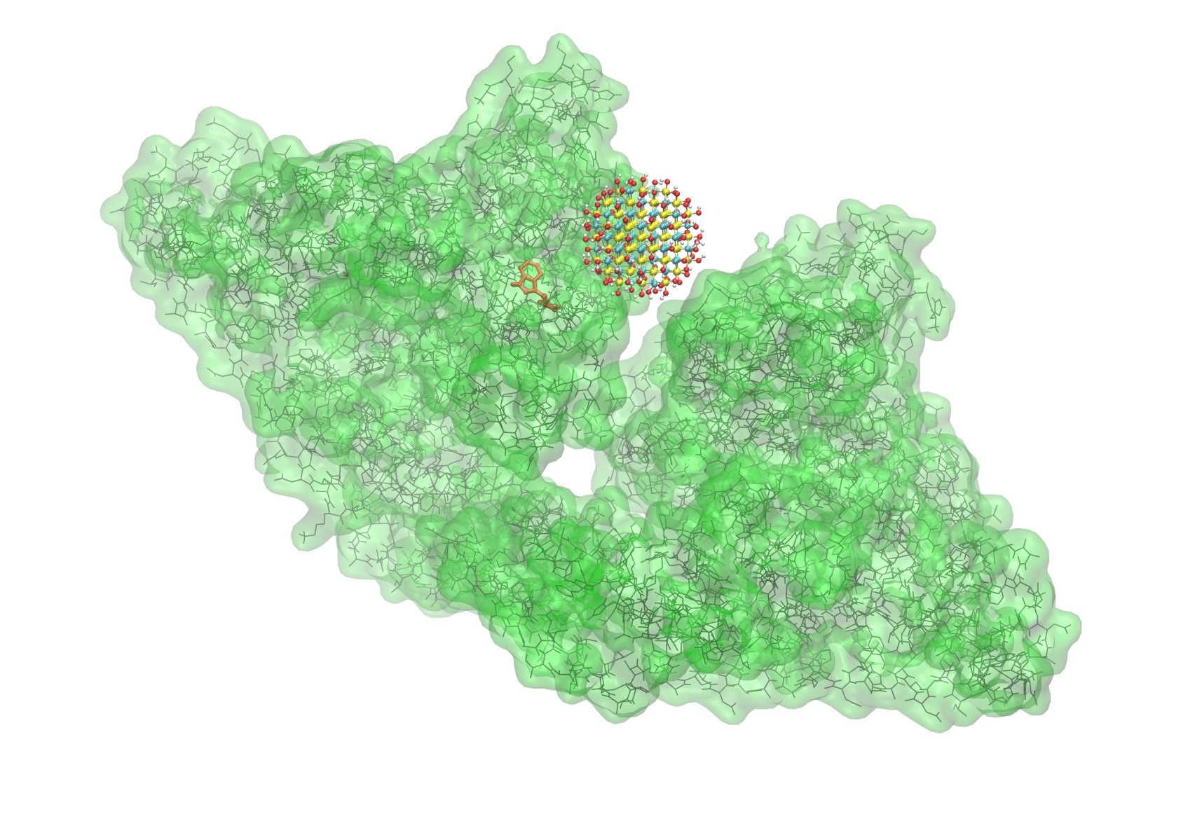
Figure 1. Binding between BSA molecule (large greenish molecule) and ultrasmall silicon carbide nanoparticle (red and yellow balls and stick spherical structure).
Significant results have been achieved in the research of solid-state quantum bits, which are the building blocks of a future implementation of the quantum computer. Diamond is a known host of solid state qubits and single photon emitters. Nitrogen-vacancy center (NV) stands out among these qubits in terms of robustness of optical spin readout and initialization. The microscopic mechanism behind the observed optical spin polarization was revealed by ab initio first principles calculations. A new method was developed and implemented to describe the so-called highly correlated electronic states in this and similar quantum bits that play a crucial role in the spin polarization process. Furthermore, the interaction between nearby NV quantum bit and acceptor defects was analyzed by the use of first principles wavefunctions, and a novel mechanism for the decoherence of the quantum bit was revealed that may play an important role in the properties of near-surface NV quantum sensors. In addition, the ab initio magneto-optical spectrum of Group-IV--Vacancy color centers was calculated in diamond, and a new spin Hamiltonian was established in which the electron spin and the phonons are strongly coupled (see Fig. 2) that has an impact in the quantum communication applications of these quantum bits.
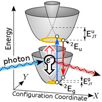
Figure 2. Schematic diagram of the photoexcitation of the negatively charged Group-IV—vacancy color centers in diamond. The Jahn-Teller unstable ground state (2Eg) state is photoexcited to the Jahn-Teller unstable excited state (2Eu) by absorbing a photon, and emits a redshifted photon in the decay process. The so-called Jahn-Teller energy (EJT) in the corresponding states is also depicted.
Furthermore, we studied nanosystems that are promising in biomarker and solar cell applications. The silicon nanoparticles (Si NPs) are very promising in various emerging technologies and for fundamental quantum studies of semiconductor nanocrystals. Heavily boron and phosphorus codoped fluorescent Si NPs can be fabricated with diameters of a few nanometers. However, very little is understood about the structure and origin of their vibration and optical spectra of these NPs. By means of first principles simulations, various spectroscopic quantities can be computed and compared to the corresponding experimental data. We characterized the size dependent photoluminescence and Raman spectra of dopant-free Si NPs and found good agreement with the experiments (see Fig. 3). Based on these encouraging results, we utilized the same methodology to study the Raman and PL spectra of 10 randomly generated heavily co-doped Si NP models (where we have chosen stable dopant configurations), and found that the results are in good agreement with the experimental spectra. These results imply that we could identify the dopant configurations in small Si NPs that are responsible for the observed photoluminescence, infrared vibration and Raman spectra.
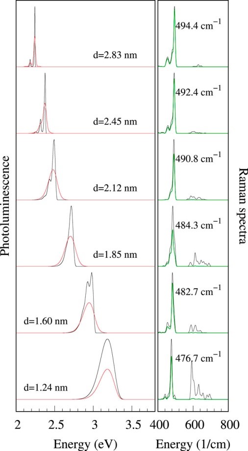
Figure 3. The calculated photoluminescence emission spectra and resonant Raman spectra of hydrogen-terminated, pristine Si nanocrystals with diameters in the region of 1.1-2.8 nm. For the PL spectra, black and red curves correspond to 0 K and 300 K, respectively. For the Raman spectra, black curves correspond to the full spectra, while green curves correspond to the projected Raman spectra where the outermost layer of Si atoms and H atoms is excluded from the projection.
2017
Design and fabrication of semiconductor nanostructures for bioimaging, quantum computing and 3rd generation photovoltaics. — The research team is active in three main different fields: develop new type of i) biomarkers, ii) quantum bits for quantum computation, and iii) 3rd generation solar cells. Next, we summarize our important achievements.
Development of biomarker systems. — Biologists urgently need biomarker systems which trace, e.g., cancer cells in the blood stream or provide fluorescent signals depending on the activity of neurons in brain. Such systems have been developed so far, but most of them are either unstable or toxic, thus they are not suitable for therapy. Our Semiconductor Nanostructures Research Group is, however, seeking such solutions that can be applied in vivo. Molecular-sized colloidal SiC nanoparticles are very promising candidates to realize bioinert non-perturbative fluorescent nanoparticles for in vivo bioimaging. These SiC nanoparticles are prepared by wet chemical etching of large SiC particles. However, the mechanism behind the etching process was far from being understood. We developed a no-photon exciton generation chemistry (NPEGEC) theory based on the experiments on SiC polytypes as a model semiconductor (see Fig. 1). Our theory applies to materials with a finite band gap. Furthermore, we could demonstrate the control over the size of SiC nanoparticles that we produce from the cubic layers of bulk cubic silicon carbide that contains hexagonal inclusions.
Nitrogen vacancy center (NV). — Significant results have been achieved in the research of solid-state quantum bits, which are the building blocks of a future implementation of the quantum computer. Diamond is a known host of solid state qubits and single photon emitters. NV center stands out among these qubits in terms of robustness of optical spin readout and initialization. The optical readout of electron spin is based on the intersystem crossing (ISC) between the optically active triplet states and the dark singlet states. However, the intricate details about the ISC processes were not fully understood. By combining the theory of dynamic Jahn-Teller system and first principles calculations, we could identify the ISC routes and their rates for the transition between the excited state triplet and a nearby singlet state (see Fig. 2).
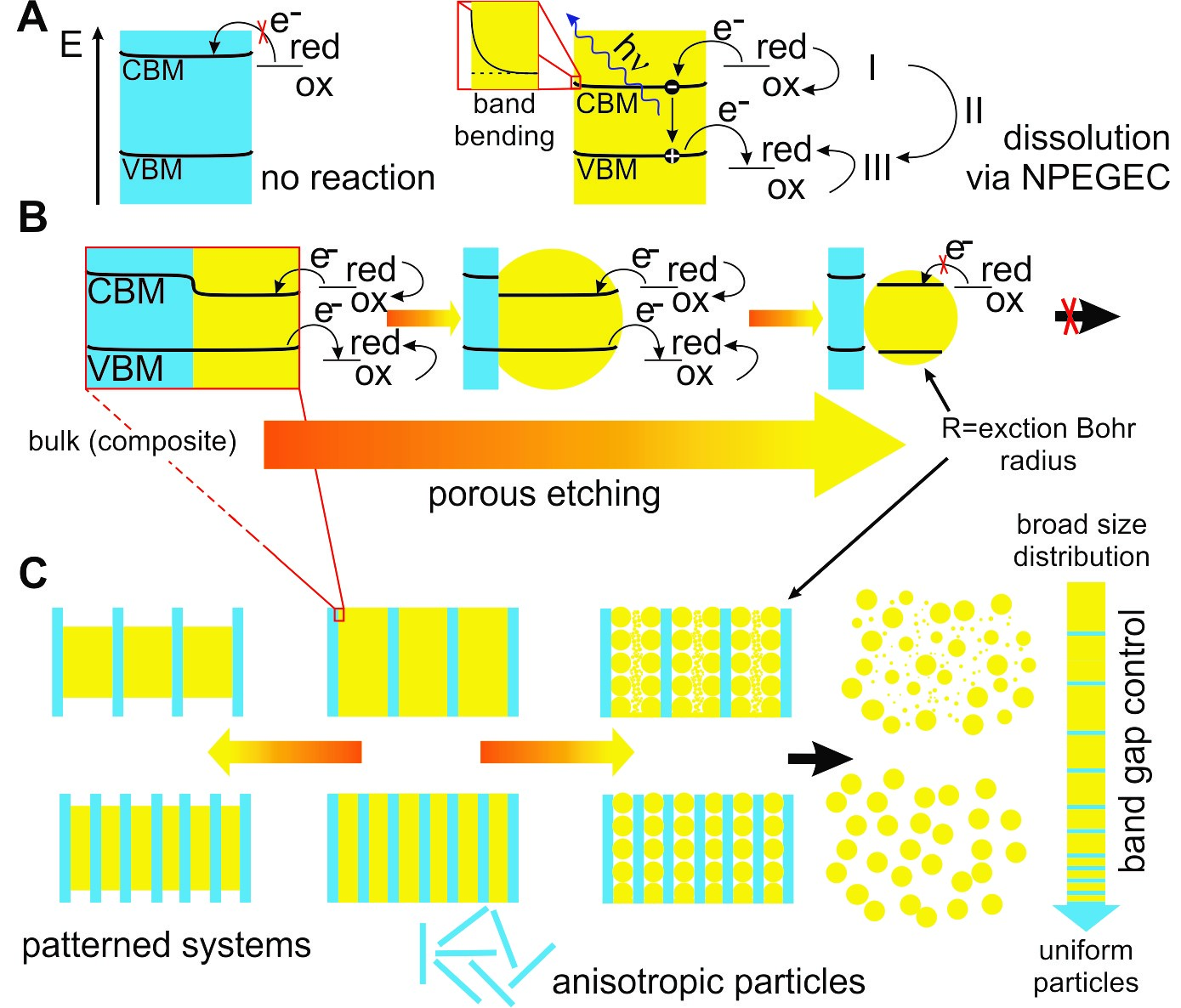
Figure 1. The mechanism “no-photon exciton generation chemistry” (NPEGEC) for stain etching of semiconductors. (A) The blue region depicts a semiconductor with a larger band gap that is resistive against etching while the yellow region represents a suitable material. A redox couple with redox potential higher (more negative) than the conduction band minimum (CBM) energy can inject electrons into the conduction band (I). The oxidized molecule itself, or the molecule formed after further transformation in the solution (II) can inject holes into the valence band (VB) with a maximum energy of VBM (III). The generated excitons can recombine with photon emission with energy h v or can lead to material dissolution. (B) In a material with spatially varying band structure selective etching is possible. The exciton Bohr radius limits the radius (R) of the final nanoparticle. (C) Patterned band structure in a macroscopic material can serve as a template for various nanostructures including patterned nanowires, anisotropic or uniform particles.
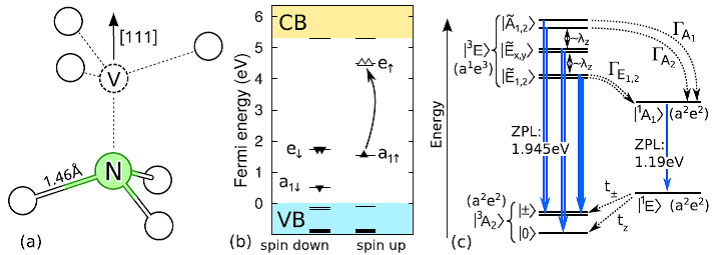
Figure 2. NV center in diamond. (a) Schematic diagram of the structure of the negatively charged defect with the optimized carbon-nitrogen bond length. The symmetry axis of the defect in the diamond lattice is shown. (b) The calculated defect levels in the gap are depicted in the ground state where the curved arrow symbolizes the SCF procedure for creating the triplet excited state. The e states are double degenerate. VB and CB correspond to valence and conduction bands, respectively. (c) The corresponding ground state and excited states are shown as well as the optical electron spin polarization cycle. The spin-orbit splitting λz is depicted that separates the sublevels in the triplet 3E excited state. The corresponding intersystem crossing rates between the 3E substates (˜A1,2, ˜E1,2 double group representations) and the singlet 1A1 are labeled by . The tilde labels the vibronic nature of these states. The intersystem crossing (t± and tz ) from the 1E to the triplet ground state is shown for the sake of completeness and closes the spin polarization cycle.
The diamond NV center can be used as a nanoscale sensor when engineered close to the diamond surface. However, the surface termination of diamond can affect the charge state and photo-stability of NV center that may compromise the sensitivity of NV center. We predict from first principles calculations that nitrogen-terminated (111) diamond would be ideal to maximize the sensitivity of near-surface NV centers (see Fig. 3). Furthermore, the array of I=1 nuclear spins of 14N isotopes on the surface can used to realize a quantum simulator of special spin systems.
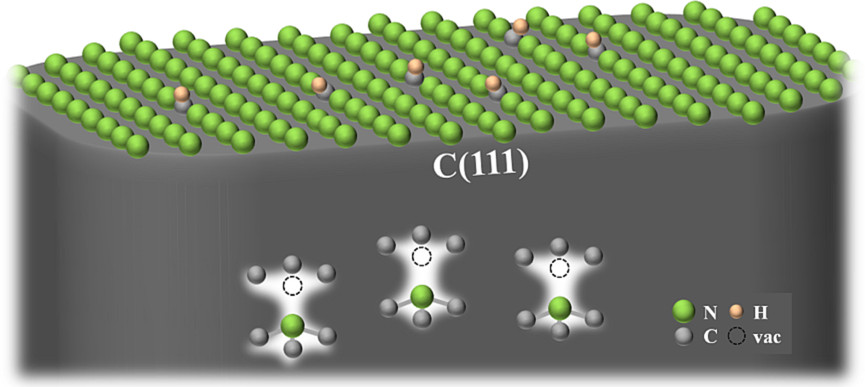
Figure 3. The (111) surface of diamond terminated with nitrogen atoms. Nitrogen vacancy centers below the terminated surface enjoy a near-bulk physical environment, e.g. long spin coherence time, which makes them useful for quantum bit and nanometrological applications.
Divacancy defect in SiC. — Another prominent solid state qubit candidate is the so-called divacancy defect in SiC which has a high-electron-spin ground state. Divacancy qubit can be formed in cubic and hexagonal polytypes, however, the key magneto-optical parameters and rates were not known for these qubits. In collaboration with the Awschalom group at Chicago University, we characterized thoroughly these qubits (see Fig. 4). We found that an efficient spin-to-photon interface can be realized by these divacancy qubits at cryogenic temperature and resonant optical excitation. Furthermore, we identified a room temperature qubit in hexagonal SiC as Si-vacancy at the so-called cubic site in hexagonal SiC by means of first principles calculations. This Si-vacancy qubit has a great potential in thermometry and magnetometry applications at the nanoscale.
Furthermore, we studied nanosystems that are promising in biomarker and solar cell applications. The silicon nanoparticles (Si NPs) are very promising in various emerging technologies and for fundamental quantum studies of semiconductor nanocrystals. Heavily boron and phosphorus codoped fluorescent Si NPs can be fabricated with diameters of a few nanometers. However, very little is understood about the structure and origin of the fluorescence of these NPs. We performed a systematic time-dependent density functional study of hundreds of codoped Si NPs representing millions of configurations. We identified the most stable dopant configurations and a correlation between these configurations and their optical gaps. We find that particular dopant configurations result in emission in the second biological window, which makes these nanoparticles viable for deep-tissue bioimaging applications. We also found that the radiative lifetime of Si NPs is intrinsically long, thus the electron-hole pairs generated by illumination can principally be separated. This concludes that heavily doped Si NPs can be applied as an absorbant for Si based solar cells.
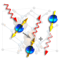
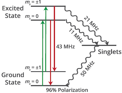
Figure 4. Dynamical model of the 3C-SiC divacancy. Up: An artistic view about the optical spin polarization of divacancy spins. Down: Diagram of the levels and major rates in the five-level rate-equation model. The transition rates and ground-state spin polarization are inferred from the combination of experimental data, group theory considerations and input from first principles calculations.