MTA Kiváló Kutatóhely
Hamburget Menu MTA.hu
  • MTA.hu főoldal
  • MTA tudományos hírek
  • MTA pályázatok
  • English
  • Hungarian
Címlap
HUN-REN Wigner Fizikai Kutatóközpont
ELKH ELKH

Main navigation

  • Rólunk
    • Vezetőség és Titkárok
    • Történet
    • Misszió és Évkönyv
    • Kutatóintézeti stratégia
    • MTA Kiváló Kutatóhely
    • Büszkeségeink
    • Közérdekű adatok
    • Alumni
  • Hírek
    • Hírek
    • Intézeti hírek
    • Állások
    • Médiamegjelenések
  • Kutatás
    • Kutatócsoportok
    • Infrastruktúra
    • Nemzeti és kutatólaboratóriumok
    • Nyitott laboratóriumok
    • Futó projektek
  • Oktatás
    • Egyetemi kurzusok
    • OTDK eredmények
    • Szakmai gyakorlat
    • Nyílt napok, diákműhelyek
    • Középiskolásoknak, tanároknak
    • PhD képzés
    • Wigner Kollokvium
  • Kommunikáció
    • Médiatár
    • Brosúrák
    • Letölthető logók
    • Sajtóközlemények
    • Ismeretterjesztés
    • Kutatók éjszakája
    • Könyvkiadás
    • Wigner Café
  • Intranet
  • Kapcsolat

Félvezető Nanoszerkezetek "Lendület" Kutatócsoport

2023


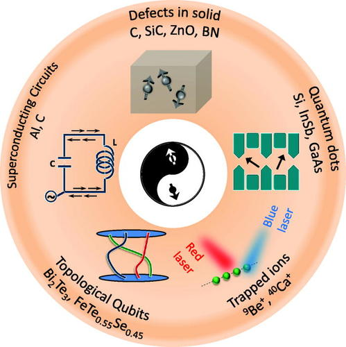
In 2023, our research group has made further substantial steps towards developing elementary hardware elements for quantum information processing. These elements are solid-state quantum bits, in most cases point defects which show magneto-optical behavior which can be harnessed to store and process quantum information. A proper investigation of such systems include their precise physical description, as for both their actual molecular structure and electronic system properties, as well as proposing a set of so-called quantum protocols which make them really usable as quantum bits, and finally validating their fundamental chemical and engineering properties for the usage in real quantum information processing environments. In almost every case, these systems are also promising candidates for nanometrology (nanosensing, biosensing) applications, as the physics of these two fields are closely related. We executed ab initio calculations on modeling the qubits by KIFÜ high-performance computing units as well as our local high performance computation cluster. 

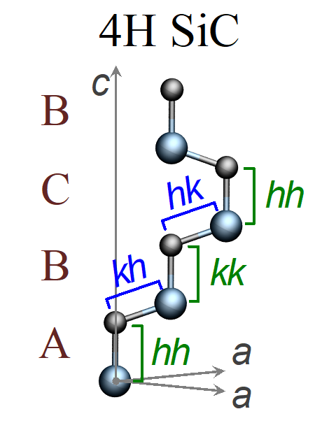
Formation of G-center in silicon. Thermal equilibrium is reached when the system assumes its lowest energy. This can be hindered by kinetic reasons; however, it is a general assumption that the ground state can be eventually reached. Here, we show that this is not always necessarily the case. Carbon pairs in silicon have at least three different configurations, one of them (B-configuration) is the G photoluminescence center. Experiments revealed a bistable nature with the A-configuration (Fig. A). Electronic structure calculations predicted that the C-configuration is the real ground state; however, no experimental evidence was found for its existence. Our calculations show that the formation of the A- and B-configurations is strongly favored over the most stable C-configuration which cannot be realized in a detectable amount before the pair dissociates. Our results demonstrate that automatized search for complex defects consisting of only the thermodynamically most stable configurations may overlook key candidates for quantum technology applications. 
 

kvantum


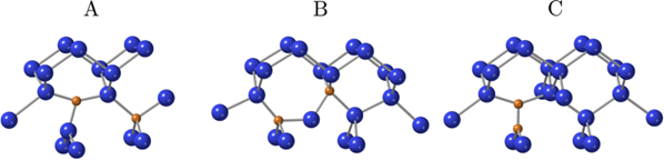
Fig. A. A, B, and C label the three configurations identified in prior studies. Brown and blues spheres are the carbon and silicon atoms, respectively. The figures are made by Crystal MakerTM.

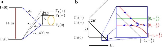
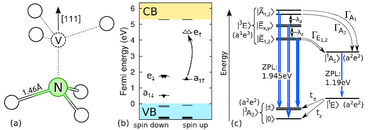
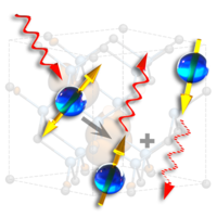
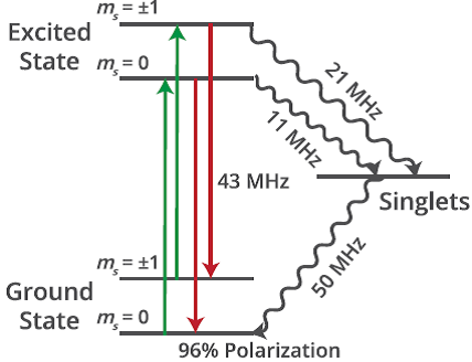
Diamond NV center spin-phonon interactions. Spin-lattice relaxation within the diamond nitrogen-vacancy (NV) center’s electronic ground-state spin triplet limits its coherence times, and thereby impacts its performance in quantum applications. Our collaborators observed the relaxation rates on the NV center’s |ms=0⟩↔|ms=±1⟩ and |ms=−1⟩↔|ms=+1⟩ transitions as a function of temperature from 9 to 474 K in high-purity samples. We showed that the temperature dependencies of the rates are reproduced by our ab initio theory of Raman scattering due to second-order spin-phonon interactions which is generally applicable to other defect spin systems [B]. We developed a theory about the nuclear spin relaxation under resonant excitation to polarize the 14N host, which our collaborator then prove beneficial for spin magnetometry in experiments [C]. The nuclear spin relaxation is mediated by the electron-phonon coupling in the electronic excited state according to our theory.

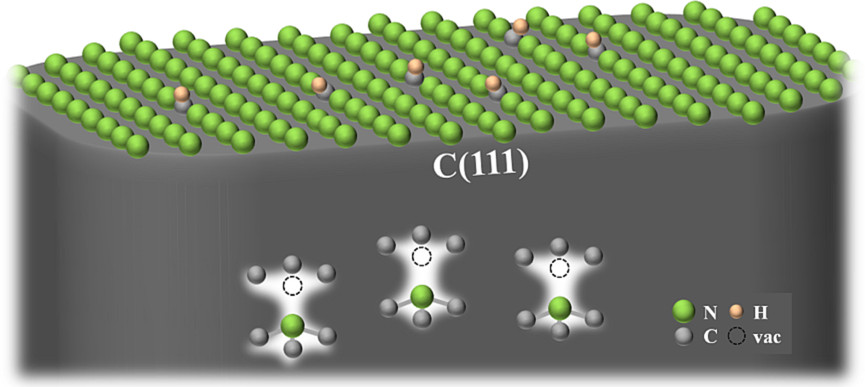
Diamond NV centers close to the surface.

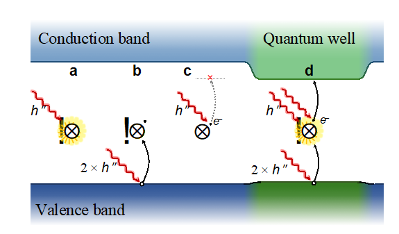
Near-surface negatively charged nitrogen vacancy (NV) centers hold excellent promise for nanoscale magnetic imaging and quantum sensing. However, they often experience charge-state instabilities, leading to strongly reduced fluorescence and NV coherence time, which negatively impact magnetic imaging sensitivity. This occurs even more severely at 4 K and ultrahigh vacuum (UHV, p = 2 × 10⁻¹⁰ mbar). Our collaborators demonstrate that in situ adsorption of H2O on the diamond surface allows the partial recovery of the shallow NV sensors. Our band-bending calculations showed that controlled surface treatments are essential for implementing NV-based quantum sensing protocols under cryogenic UHV conditions [D]. Molecules or ions with unpaired electronic spins are typically probed by their influence on the NV center’s spin relaxation. Whereas it is well-known that paramagnetic ions reduce the NV center’s relaxation time (T1), our collaborators reported on the opposite effect for diamagnetic ions. To elucidate the underlying mechanism of this surprising effect, single and double quantum NV experiments are performed, which indicate a reduction of magnetic and electric noise in the presence of diamagnetic electrolytes. Our ab initio simulations shows that a change in the interfacial band bending due to the formation of an electric double layer leads to a stabilization of fluctuating charges at the interface of an oxidized diamond [E].

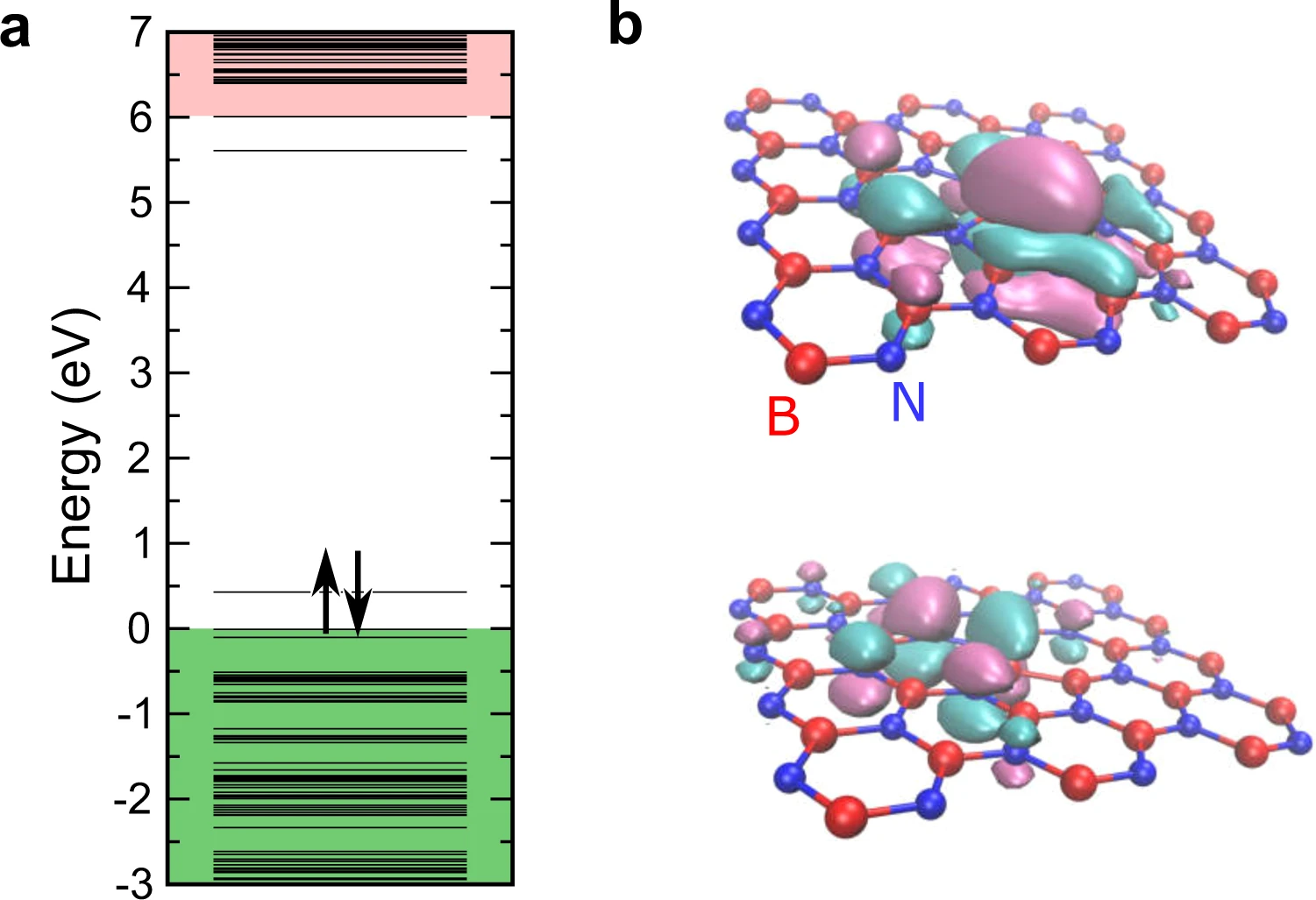
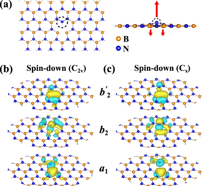
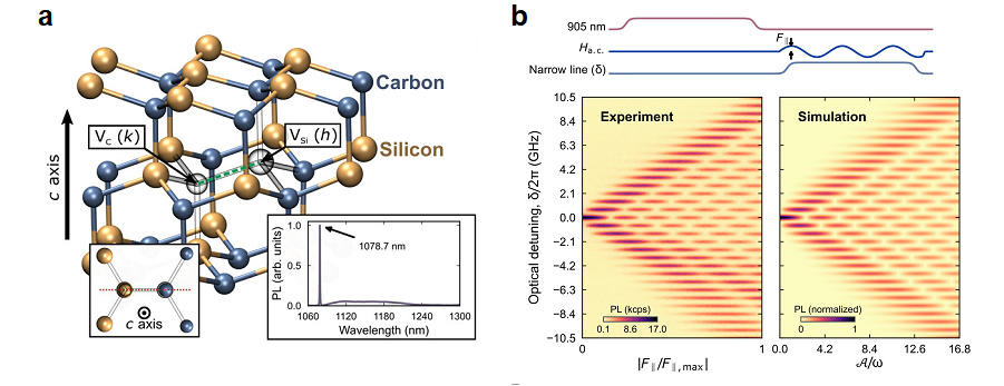
Hexagonal boron nitride boron-vacancy spin’s coupling to external fields. Hexagonal boron nitride (hBN) has recently been demonstrated to contain optically polarized and detected electron spins that can be utilized for implementing qubits and quantum sensors in nanolayered-devices. The boron-vacancy spin defect in hexagonal boron nitride (hBN) has a great potential as a quantum sensor in a two-dimensional material that can directly probe various external perturbations in atomic-scale proximity to the quantum sensing layer. Here, we apply first-principles calculations to determine the coupling of the electronic spin to strain and electric fields. Our work unraveled the interplay between local piezoelectric and elastic effects contributing to the final response to the electric fields. The theoretical predictions are then used to analyze optically detected magnetic resonance (ODMR) spectra recorded on hBN crystals containing different densities of centers. We prove that the orthorhombic zero-field splitting parameter results from local electric fields produced by surrounding charge defects [F]. These results explain the observations of boron-vacancy spin defects in few-atomic-layers thick hexagonal boron nitride [G].

References:
[A] https://www.nature.com/articles/s41467-023-36090-2 
[B] https://journals.aps.org/prl/abstract/10.1103/PhysRevLett.130.256903
[C] https://journals.aps.org/prl/abstract/10.1103/PhysRevLett.131.236901
[D] https://pubs.acs.org/doi/10.1021/acs.nanolett.2c04733
[E] https://pubs.acs.org/doi/10.1021/acsnano.3c01298
[F] https://www.nature.com/articles/s41524-023-01111-7
[G] https://journals.aps.org/prl/abstract/10.1103/PhysRevLett.131.116902
 

2022

In 2022, our research group has made further substantial steps towards developing elementary hardware elements for quantum information processing. These elements are solid-state quantum bits, in most cases point defects which show magneto-optical behaviour which can be harnessed to store and process quantum information. A proper investigation of such systems include their precise physical description, as for both their actual molecular structure and electronic system properties, as well as proposing a set of so-called quantum protocols which make them really usable as quantum bits, and finally validating their fundamental chemical and engineering properties for the usage in real quantum information processing environments. In almost every case, these systems are also promising candidates for nanometrology (nanosensing, biosensing) applications, as the physics of these two fields are closely related. We executed ab initio calculations on modeling the qubits by KIFÜ high-performance computing units.

An L-band emitter with quantum memory in silicon. Fluorescent centres in silicon have recently attracted great interest, owing to their remarkable properties for quantum technology. We have demonstrated [A] that the C centre in silicon can realise an optically readable quantum register in the L-band wavelength region where the transmission losses in commercial optical fibres are minimal. As an important consequence, our in-depth theoretical characterisation confirms the assignment of the C centre to the carbon-oxygen interstitial pair defect. We further explored its magneto-optical properties, such as hyperfine and spin-orbit coupling constants from first principles calculations, which are crucial for tight control of the quantum states of the triplet electron spin. Based on this data, we set up quantum optics protocols to initialise and read out the quantum states of the electron spin, and realise a quantum memory by transferring quantum information from the electron spin to proximate 29Si nuclear spins. Our findings establish an optically readable long-living quantum memory in silicon where the scalability of qubits may be achieved by CMOS-compatible technology.

nanostructure 1

Fig. A. The quantum protocol proposed by us for the C centre is based on the electronic structure shown in (a). The red and blue arrows show fluorescence and phosphorescence, the blue dashed arrow highlights the spin-selective intersystem crossing (ISC) that leads to the main contribution to phosphorescence. Orange lines correspond to coherent spin control using microwave excitation. The spin-selective ISC initialises the bright |0⟩ spin state. Magnetic field dependence of the triplet electronic and doublet nuclear spin levels labelled by |mS,mI⟩ is in (b). Procedure for the Landau-Zener transition is highlighted for negative hyperfine coupling parameters. The initial superposition of electronic states (green and red with spins up and down) is transferred to the coherent superposition of nuclear states. The degenerate hyperfine levels (with zero nuclear spin) are separated for the sake of clarity.

Coherent dynamics of multi-spin V−B center in hexagonal boron nitride. Hexagonal boron nitride (hBN) has recently been demonstrated to contain optically polarized and detected electron spins that can be utilized for implementing qubits and quantum sensors in nanolayered-devices. Understanding the coherent dynamics of microwave driven spins in hBN is of crucial importance for advancing these emerging new technologies. In our investigation, we have demonstrated and studied the Rabi oscillation and related phenomena of a negatively charged boron vacancy (VB−) spin ensemble in hBN. It is an important result of our calculations that VB− spins have different dynamics at weak and strong magnetic fields. In the former case the defect behaves like a single-electron-spin system, while in the latter case it behaves like a multi-spin system exhibiting multiple-frequency dynamical oscillation as a beat in the Ramsey fringes (see fig. B). We have also carried out theoretical simulations for the spin dynamics of VB− and revealed that the nuclear spins can be driven via the strong electron-nuclear coupling existing in VB− center, which can be modulated by the stationary magnetic field and the microwave field.

nanosturcture 2

Fig. B. The Ramsey beat as a reaction to a 2200 MHz microwave irradiation in (a) in a stationary magnetic field of 44 mT. The fitted red oscillation in (b) is a superposition of three decaying frequencies two of which clearly form a beat.

Optimization of chromium-doped zinc gallate nanocrystals for strong near-infrared emission by annealing. Chromium-doped spinel (MgAl2O4) crystals show long-lasting emissions in the near-infrared wavelength region. The emission can be activated by X-ray or ultraviolet–visible (UV–visible) light. Such properties make this material a promising candidate for background-free deep-tissue bioimaging, photodynamic or photon-induced therapy, and other applications. Our experimental group has applied hydrothermal synthesis for the preparation of Cr-doped zinc gallate (ZnGa2O4) nanoparticles of small sizes with around 10 nm in diameter, [C] which has the potential to be intravenously introduced to patients. We have found that annealing of the as-prepared nanoparticles at 800 °C yields an order of magnitude increase in the emission intensity in the near-infrared wavelength region upon X-ray exposure with favorable long-lasting photoluminescence, which may be directly employed for deep-tissue cancer treatments when combined with IR700-mAb conjugate drug agents. We have studied and discussed the effect of annealing on the structural changes and the evolution of Cr defects of 10 nm Cr-doped zinc gallate nanoparticles by imaging techniques and monitoring their magneto-optical signals (fig. C).

nanosturcure 3

Fig. C. We have calculated the (b) crystal sizes and (c) bond lengths (with reference values in gray) from the (a) X-ray diffraction data of Cr-doped zinc gallate (ZGO:Cr) by Rietveld analysis. Error bars for crystallite size represented the variation in the particle size in the repeated experiments in (b). Part (d) shows scanning electron microscopy images and ZGO:Cr nanoparticles with particle size distribution and (e) is their Raman spectra as a function of annealing temperature. Raman active peaks are labeled in black.


Carbon defect qubit in two-dimensional WS2. Identifying and fabricating defect qubits in two-dimensional semiconductors are of great interest in exploring candidates for quantum information and sensing applications. A milestone has been recently achieved by demonstrating that a single defect, a carbon atom substituting a sulphur atom in single-layer tungsten disulphide (CS–, see fig. D), can be engineered on demand at atomic size level precision, which holds a promise for a scalable and addressable unit. It is an immediate quest to reveal its potential as a qubit. To this end, we have determined its electronic structure and optical properties using first-principles calculations. [D] We identify the fingerprint of the neutral charge state of the defect in the scanning tunnelling spectrum. In the neutral defect, the giant spin-orbit coupling mixes the singlet and triplet excited states resulting in phosphorescence at the telecom band, which can be used to read out the spin state, and coherent driving with microwave excitation is also viable. Our results establish a scalable qubit in a two-dimensional material with a spin-photon interface at the telecom wavelength region.

nanostructure 4

Fig. D. The CS– defect seen from within the WS layer (a) and its electronic structure in the ground state (b) with the modifying effect of spin-orbit coupling also shown (c). The spatial wavefunctions of the denoted defect levels are also shown in (d).

References:
[A] https://www.nature.com/articles/s41524-022-00957-7
[B] https://www.nature.com/articles/s41467-022-33399-2
[C] https://pubs.acs.org/doi/10.1021/acsanm.2c01156
[D] https://www.nature.com/articles/s41467-022-28876-7

2020

The major thrust in our group is the design, preparation, characterization and application of solid state defect qubits. As we have recently described in our comprehensive review paper [1], various systems are under intense research for realization of controllable qubit systems (see Fig. 1). We focus our research on solid-state spins and emitters in several leading host materials, including diamond, silicon carbide, boron nitride, silicon, two-dimensional semiconductors, and other materials. We characterize the defect qubits by first principles theory and quantum optics measurements in our laboratory. We emphasize some key results reported in 2020.
 

félvezető nanoszerkezetek 1

Figure 1. Implementations of macroscopically controllable two-state spin systems, the so-called qubits

2. Optically Detected Magnetic Resonance (ODMR) in Neutral Silicon Vacancy Centers in Diamond via Bound Exciton States. Neutral silicon vacancy (SiV0) centers in diamond are promising candidates for quantum networks because of their excellent optical properties and long spin coherence times. However, spin-dependent fluorescence in such defects has been elusive due to poor understanding of the excited state fine structure and limited off-resonant spin polarization. We reported the realization of optically detected magnetic resonance and coherent control of SiV0 centers at cryogenic temperatures in cooperation with Princeton University, enabled by efficient optical spin polarization via previously unreported higher-lying excited states. We assign these states as bound exciton states using group theory and density functional theory. These bound exciton states enable new control schemes for SiV0 as well as other emerging defect systems.

3. Novel implementations of point-defect qubits in two-dimensional hexagonal boron nitride. Our research group, like the whole world, focuses mostly on diamond and silicon carbide when solid-state qubits come into question. Many of our papers, however, dealt with boron-nitride-based systems in 2020, a new, emerging type of point-defect quantum nanosystems. First, we mention a study [3] in which we dealt with Stone–Walls defects, which can be found e.g. near the grain boundaries of the two-dimensional hexagonal boron nitride. We show by means of first principles density functional theory calculations that the pentagon–heptagon Stone–Wales defect (Fig. 2) is an ultraviolet emitter and its optical properties closely follow the characteristics of a 4.08-eV quantum emitter, often observed in polycrystalline hexagonal boron nitride. We also show that the square–octagon Stone–Wales line defects are optically active in the ultraviolet region with varying gaps depending on their density in hexagonal boron nitride. Our results may introduce a paradigm shift in the identification of fluorescent centres in this material.


félvezető nanoszerkezetek 2

Figure 2. System of electronic levels in the pentagon-heptagon Stone–Walls defect in boron nitride, as well as the visualization of the highest occupied, and the lowest unoccupied electronic orbital.

In another paper, [4] we study the effect of strain on the physical properties of the nitrogen antisite-boron vacancy pair (VN-NB, see Fig 3.) in hexagonal boron nitride (h-BN), a color center that may be employed as a quantum bit in a two-dimensional material. With group theory and ab initio analysis we show that strong electron–phonon coupling plays a key role in the optical activation of this color center. We find a giant shift on the zero-phonon-line (ZPL) emission of the nitrogen antisite-vacancy pair defect upon applying strain that is typical of h-BN samples. Our results provide a plausible explanation for the experimental observation of quantum emitters with similar optical properties but widely scattered ZPL wavelengths and the experimentally observed dependence of the ZPL on the strain.

félvezető nanoszerkezetek 3

Figure 3. Change of symmetries in the VN-NB point defect in boron nitride by motion of atoms perpendicular to the hexagonal plane. The relevant electronic wavefunctions change accordingly.

Staying with boron nitride for one more important paper, [5] we identify highly correlated orbitals coupled with phonons in two dimension to explain the paramagnetic and optically active boron vacancy (VB) in hexagonal boron nitride by first principles methods, which are responsible for recently observed optically detected magnetic resonance signal. We report ab initio analysis of the correlated electronic structure of this center by density matrix renormalization group and Kohn-Sham density functional theory methods, and provide a complete description of the optical spin polarization and spin dependent luminescence of the defect. Our findings pave the way toward advancing the identification and characterization of room temperature quantum bits in two-dimensional solids.

4. Manufacturing Room-Temperature Defect Qubits in Ultrasmall Nanocrystals. There is an urgent quest for room-temperature qubits in nanometer-sized, ultrasmall nanocrystals for quantum biosensing, hyperpolarization of biomolecules, and quantum information processing. Thus far, the preparation of such qubits at the nanoscale has remained futile. In this paper, [6] we present a synthesis method that avoids any interaction of the solid with high-energy particles and uses self-propagated high-temperature synthesis with a subsequent electrochemical method, the “no-photon exciton generation chemistry” to produce room-temperature qubits in ultrasmall nanocrystals of sizes down to 3 nm with high yield. We first create the host silicon carbide (SiC) crystallites by high-temperature synthesis and then apply wet chemical etching, which results in ultrasmall SiC nanocrystals and facilitates the creation of thermally stable defect qubits in the material. We demonstrate room-temperature optically detected magnetic resonance signal of divacancy qubits with 3.5% contrast from these nanoparticles with emission wavelengths falling in the second biological window (1000–1380 nm). These results constitute the formation of nonperturbative bioagents for quantum sensing and efficient hyperpolarization.

félvezető nanoszerkezetek 4

Figure 4. The process of high-yield manufacturing of ultrasmall nanoparticles with point-defect qubits


[1] https://doi.org/10.1063%2F5.0006075
[2] https://doi.org/10.1103%2FPhysRevLett.125.237402
[3] https://doi.org/10.1038%2Fs41524-020-00451-y
[4] https://doi.org/10.1038%2Fs41534-020-00312-y
[5] https://doi.org/10.1038%2Fs41524-020-0305-x
[6] https://doi.org/10.1021%2Facs.jpclett.0c00052

2019

The research team is active in three main different fields: developing new type of i) biomarkers, ii) quantum bits for quantum information processing, and iii) 3rd generation solar cells. István Balogh, Balázs Juhász, Péter Rózsa, János Tamási, Dávid Veres, Ádám Viszoki, Dóra Zalka and Szabolcs Czene mediate the experiments as laboratory assistants. Hanen Hamdi, Vladimir Verkhovlyuk, Philipp Auburger, Anton Pershin and Szabolcs Czene has joined the group in 2019.

Next, we give some highlights of our achievements last year.

Qubits are two-state quantum systems with a low level of interaction with their environments, but still with the ability of being controlled. Paramagnetic point defects in semiconductors are an example, and moreover, if they are also fluorescent as well as their fluorescence intensity depends on the spin state (optically detected magnetic resonance, ODMR), they become spin-optical interfaces, i.e. their spin state can be modified and tested with optical methods. The most interesting such systems are embedded in host materials which have widespread use in semiconductor industry.

Ádám Gali has published back in 2009 his theoretical result that silicon carbide (SiC), a wide-gap semiconductor used in power electronics may contain a point defect of the above type. This point defect is the divacancy defect, an S = 1 paramagnetic qubit with luminescence in the 1100–1300 nanometer infrared range, which is formed when a carbon atom and an adjacent silicon atom are missing from the host lattice. In a tight cooperation with the group of David D. Awschalom (The University of Chicago), our group has considerably contributed to understanding the physics of the divacancy point defect in silicon carbide last year. In these investigations, the host material is 4H-SiC, which is the industrially most-used SiC polytype.

The divacancy point defect can be aligned in four non-equivalent ways in the perfect 4H-SiC layer structure (see fig. 1). Two (PL1, PL2) are high-symmetry (showing threefold rotational symmetry just like in a diamond lattice), and two (PL3, PL4) are low-symmetry (showing only one mirroring symmetry). In an earlier publication of the Awschalom group, experimental results showed two further types (PL5 and PL6 centres with divacancy-like signals).

S-D2019-1

Figure 1. The stacking sequence of 4H-SiC. Every layer is classified as h (hexagonal) or k (cubic) based on its position with respect to the underlying one. The cubic position ensures higher symmetry (locally a diamond-like cubic lattice) at atomic positions. If we eliminate an adjacent pair of a C and a Si atom to generate a divacancy, the adjacent positions in question can be labelled kk, kh, hk, and hh.

Mainly as a work of Viktor Ivády, we have explained PL5 and PL6 with high-precision density-functional-theory calculations . They are divacancy point defects, as previously thought, but embedded in a stacking fault of the 4H-SiC host which is an additional cubic layer instead of a hexagonal one. This stacking fault results in a 0.3 eV deep quantum well in the conduction band, which can trap electrons, and largely alter the photostability of the point defect, which will be an extremely important further property of PL5 and PL6.

This is because divacancy defects in SiC can be ionized by sequential absorption of two photons, via the excited state we also use in their ODMR manipulation. This renders them useless as qubits, and a complicated extra machinery (including a shorter-wavelength laser) is needed to maintain their availability. As it is illustrated in Fig. 2, the PL5 and PL6 defects, however, can be de-ionized with the same wavelength we use for ODMR, and this makes them available for qubit operations almost full-time.

S-D2019-2

Figure 2. Photoexcitation pro­cesses in the PLi centres. a. These divacancy complexes show photo­luminescence. b. By absorbing two photons, the centre is ionized, and ceases being a qubit. c. Absobing an additional photon in the ionized state is not enough to get rid of the additional electron in PL1–4 cen­tres. d. Due to the lower CBM edge, an additional photon is enough for de-ionization.

Our cooperation partners at the Linköping University of Sweden have managed to create good samples with PL5 and PL6 defects, and the Chicago University partners at the Argonne National Laboratory examined these samples with their high-resolution X-ray diffraction facility. Their results confirm that PL5 and PL6 defects are associated with cubic stacking faults in 4H-SiC.

PL3 and PL4 defects have been further investigated by the Awschalom group, and they have been shown to exhibit the so-called Landau–Zener–Stückelberg (LZS) interference in the presence of alternating electric field (microwave range), at low temperature, using resonant optical excitation. This is a coherent coupling of the electron spin to the microwave field. The phenomenon has been theoretically explained by calculating the detailed electronic structure of the defect by our research group .

An interesting feature in this process is that the quantization axis of the electron spin is aligned at 70.5 degrees from the hexagonal crystal axis, and the degenerated states are split by the crystal field, which dominates spin-orbit interaction in this case. As a result, the effective model spin Hamiltonian behaves as if the spin quantization axis were a virtual rotational symmetry axis. Using this, the measured LZS interference diagram could be well explained (Fig. 3), and this gives a general strategy to investigate any low-symmetry point-defect qubit.

S-D2019-3

Figure 3. a. PL4 defect configuration in the SiC lattice. The lower right inset shows its photoluminescence spectrum with the ZPL pointed at by the arrow. b. The LZS interference pattern.

In another chief field of our activities, we use density-functional theory calculations to see if other group-IV elements (namely germanium, tin, and lead) paired with a vacancy in a colour centre exhibit similar optical properties to the silicon-vacancy centre in diamond, but with improved spin properties, that permit an economical cooling system. We have developed a new theory for understanding the interaction of light and magnetic fields with these colour centres, and we explore how the dynamical motion of the atoms strongly affects the magneto-optical properties of the defect.

S-D2019-4

Figure 4. Potential energy surfaces of a vacancy-related dimer complex in diamond. The ellipsoidal minima illustrate the dynamical Jahn-Teller orbits of atoms. Note how the potential energy map changes when the complex gets excited by a photon (or in inverse, when it goes off by emitting another during photoluminescence).

By combining our theory with density-functional theory calculations, we find that lead-vacancy colour centres should have favourable optical and spin properties for operating at room temperature. Mainly as the work of Gergő Thiering, we have developed the model of the so-called dynamical Jahn-Teller effect in these point defects, which gives strong electron-phonon coupling via the dynamic motion of atoms in these systems, (see fig. 4).

In parallel to the theoretical efforts, our experimental group in the Wigner ADMIL laboratory has managed to fabricate and test divacancy centres in tiny SiC nanoparticles. This result can be the basis for future medical applications, for example. Our researchers have filed for a patent on this model technology.

2018

Design and fabrication of semiconductor nanostructures for bioimaging, quantum computing and 3rd generation photovoltaics

The research team is active in three main different fields: developing new type of i) biomarkers, ii) quantum bits for quantum information processing, and iii) 3rd generation solar cells. Dániel Áron Major, Dániel Unyi, Balázs Juhász, Titanilla Szilvia Papp, Mátyás Mihály Rudolf and Sebestyén Szabó (BSc and MSc students in chemical engineering and physics) are also active members of the group. Five labor assistants (István Balogh, Péter Rózsa, Dávid Veres, Fanni Oláh, Dóra Zalka) mediate the experiments. Emilie Bruyer left the group in May. Nain Mukesh joint the group in July. Gergő Thiering defended his PhD thesis in December. Next, we summarize our important achievements.

Biologists urgently need biomarker systems which trace e.g. cancer cells in the blood stream or provide fluorescent signals depending on the activity of neurons in brain. Such systems have been developed so far, but most of them are either unstable or toxic, thus they are not suitable for therapy. Our Semiconductor Nanostructures Research Group is, however, seeking such solutions that can be applied in vivo. Molecular-sized colloid SiC nanoparticles are very promising candidates to realize bioinert non-perturbative fluorescent nanoparticles for in vivo bioimaging. These SiC nanoparticles are prepared by wet chemical etching of large SiC particles. Our prepared colloid SiC nanoparticles are indeed fluorescent, however, the size dependence of the fluorescent properties were not understood. By advanced wet chemical etching methods, we were able to control the size of SiC nanoparticles and monitor their optical properties by steady state and time-dependent optical methods. We found a direct evidence for transition from bulk-like to molecular-like fluorescence going from 4-6 nm to 2-4 nm sized SiC nanoparticles. Furthermore, we studied the interaction of molecular-size SiC nanoparticles and BSA proteins as a model for human HSA proteins. By combining various optical techniques and simulation methods, the binding site of ultrasmall SiC nanoparticles to the BSA molecule was identified (see Fig. 1).
ga 1
Figure 1. Binding between BSA molecule (large greenish molecule) and ultrasmall silicon carbide nanoparticle (red and yellow balls and stick spherical structure).

Significant results have been achieved in the research of solid-state quantum bits, which are the building blocks of a future implementation of the quantum computer. Diamond is a known host of solid state qubits and single photon emitters. Nitrogen-vacancy center (NV) stands out among these qubits in terms of robustness of optical spin readout and initialization. The microscopic mechanism behind the observed optical spin polarization was revealed by ab initio first principles calculations. A new method was developed and implemented to describe the so-called highly correlated electronic states in this and similar quantum bits that play a crucial role in the spin polarization process. Furthermore, the interaction between nearby NV quantum bit and acceptor defects was analyzed by the use of first principles wavefunctions, and a novel mechanism for the decoherence of the quantum bit was revealed that may play an important role in the properties of near-surface NV quantum sensors. In addition, the ab initio magneto-optical spectrum of Group-IV--Vacancy color centers was calculated in diamond, and a new spin Hamiltonian was established in which the electron spin and the phonons are strongly coupled (see Fig. 2) that has an impact in the quantum communication applications of these quantum bits.

ga 2

Figure 2. Schematic diagram of the photoexcitation of the negatively charged Group-IV—vacancy color centers in diamond. The Jahn-Teller unstable ground state (2Eg) state is photoexcited to the Jahn-Teller unstable excited state (2Eu) by absorbing a photon, and emits a redshifted photon in the decay process. The so-called Jahn-Teller energy (EJT) in the corresponding states is also depicted. 

Furthermore, we studied nanosystems that are promising in biomarker and solar cell applications. The silicon nanoparticles (Si NPs) are very promising in various emerging technologies and for fundamental quantum studies of semiconductor nanocrystals. Heavily boron and phosphorus codoped fluorescent Si NPs can be fabricated with diameters of a few nanometers. However, very little is understood about the structure and origin of their vibration and optical spectra of these NPs. By means of first principles simulations, various spectroscopic quantities can be computed and compared to the corresponding experimental data. We characterized the size dependent photoluminescence and Raman spectra of dopant-free Si NPs and found good agreement with the experiments (see Fig. 3). Based on these encouraging results, we utilized the same methodology to study the Raman and PL spectra of 10 randomly generated heavily co-doped Si NP models (where we have chosen stable dopant configurations), and found that the results are in good agreement with the experimental spectra. These results imply that we could identify the dopant configurations in small Si NPs that are responsible for the observed photoluminescence, infrared vibration and Raman spectra.

ga 3

Figure 3. The calculated photoluminescence emission spectra and resonant Raman spectra of hydrogen-terminated, pristine Si nanocrystals with diameters in the region of 1.1-2.8 nm. For the PL spectra, black and red curves correspond to 0 K and 300 K, respectively. For the Raman spectra, black curves correspond to the full spectra, while green curves correspond to the projected Raman spectra where the outermost layer of Si atoms and H atoms is excluded from the projection.


2017

Design and fabrication of semiconductor nanostructures for bioimaging, quantum computing and 3rd generation photovoltaics. — The research team is active in three main different fields: develop new type of i) biomarkers, ii) quantum bits for quantum computation, and iii) 3rd generation solar cells. Next, we summarize our important achievements.

Development of biomarker systems. — Biologists urgently need biomarker systems which trace, e.g., cancer cells in the blood stream or provide fluorescent signals depending on the activity of neurons in brain. Such systems have been developed so far, but most of them are either unstable or toxic, thus they are not suitable for therapy. Our Semiconductor Nanostructures Research Group is, however, seeking such solutions that can be applied in vivo. Molecular-sized colloidal SiC nanoparticles are very promising candidates to realize bioinert non-perturbative fluorescent nanoparticles for in vivo bioimaging. These SiC nanoparticles are prepared by wet chemical etching of large SiC particles. However, the mechanism behind the etching process was far from being understood. We developed a no-photon exciton generation chemistry (NPEGEC) theory based on the experiments on SiC polytypes as a model semiconductor (see Fig. 1). Our theory applies to materials with a finite band gap. Furthermore, we could demonstrate the control over the size of SiC nanoparticles that we produce from the cubic layers of bulk cubic silicon carbide that contains hexagonal inclusions.

Nitrogen vacancy center (NV). — Significant results have been achieved in the research of solid-state quantum bits, which are the building blocks of a future implementation of the quantum computer. Diamond is a known host of solid state qubits and single photon emitters. NV center stands out among these qubits in terms of robustness of optical spin readout and initialization. The optical readout of electron spin is based on the intersystem crossing (ISC) between the optically active triplet states and the dark singlet states. However, the intricate details about the ISC processes were not fully understood. By combining the theory of dynamic Jahn-Teller system and first principles calculations, we could identify the ISC routes and their rates for the transition between the excited state triplet and a nearby singlet state (see Fig. 2).

g1


Figure 1. The mechanism “no-photon exciton generation chemistry” (NPEGEC) for stain etching of semiconductors. (A) The blue region depicts a semiconductor with a larger band gap that is resistive against etching while the yellow region represents a suitable material. A redox couple with redox potential higher (more negative) than the conduction band minimum (CBM) energy can inject electrons into the conduction band (I). The oxidized molecule itself, or the molecule formed after further transformation in the solution (II) can inject holes into the valence band (VB) with a maximum energy of VBM (III). The generated excitons can recombine with photon emission with energy h v or can lead to material dissolution. (B) In a material with spatially varying band structure selective etching is possible. The exciton Bohr radius limits the radius (R) of the final nanoparticle. (C) Patterned band structure in a macroscopic material can serve as a template for various nanostructures including patterned nanowires, anisotropic or uniform particles.

g2

Figure 2. NV center in diamond. (a) Schematic diagram of the structure of the negatively charged defect with the optimized carbon-nitrogen bond length. The symmetry axis of the defect in the diamond lattice is shown. (b) The calculated defect levels in the gap are depicted in the ground state where the curved arrow symbolizes the  SCF procedure for creating the triplet excited state. The e states are double degenerate. VB and CB correspond to valence and conduction bands, respectively. (c) The corresponding ground state and excited states are shown as well as the optical electron spin polarization cycle. The spin-orbit splitting λz is depicted that separates the sublevels in the triplet 3E excited state. The corresponding intersystem crossing rates between the 3E substates (˜A1,2, ˜E1,2 double group representations) and the singlet 1A1 are labeled by  . The tilde labels the vibronic nature of these states. The intersystem crossing (t± and tz ) from the 1E to the triplet ground state is shown for the sake of completeness and closes the spin polarization cycle.

The diamond NV center can be used as a nanoscale sensor when engineered close to the diamond surface. However, the surface termination of diamond can affect the charge state and photo-stability of NV center that may compromise the sensitivity of NV center. We predict from first principles calculations that nitrogen-terminated (111) diamond would be ideal to maximize the sensitivity of near-surface NV centers (see Fig. 3). Furthermore, the array of I=1 nuclear spins of 14N isotopes on the surface can used to realize a quantum simulator of special spin systems.

g3

Figure 3. The (111) surface of diamond terminated with nitro­gen atoms. Nitrogen vacancy centers below the terminated surface enjoy a near-bulk physi­cal environment, e.g. long spin coherence time, which makes them useful for quantum bit and nanometrological applications.

Divacancy defect in SiC. — Another prominent solid state qubit candidate is the so-called divacancy defect in SiC which has a high-electron-spin ground state. Divacancy qubit can be formed in cubic and hexagonal polytypes, however, the key magneto-optical parameters and rates were not known for these qubits. In collaboration with the Awschalom group at Chicago University, we characterized thoroughly these qubits (see Fig. 4). We found that an efficient spin-to-photon interface can be realized by these divacancy qubits at cryogenic temperature and resonant optical excitation. Furthermore, we identified a room temperature qubit in hexagonal SiC as Si-vacancy at the so-called cubic site in hexagonal SiC by means of first principles calculations. This Si-vacancy qubit has a great potential in thermometry and magnetometry applications at the nanoscale.

Furthermore, we studied nanosystems that are promising in biomarker and solar cell applications. The silicon nanoparticles (Si NPs) are very promising in various emerging technologies and for fundamental quantum studies of semiconductor nanocrystals. Heavily boron and phosphorus codoped fluorescent Si NPs can be fabricated with diameters of a few nanometers. However, very little is understood about the structure and origin of the fluorescence of these NPs. We performed a systematic time-dependent density functional study of hundreds of codoped Si NPs representing millions of configurations. We identified the most stable dopant configurations and a correlation between these configurations and their optical gaps. We find that particular dopant configurations result in emission in the second biological window, which makes these nanoparticles viable for deep-tissue bioimaging applications. We also found that the radiative lifetime of Si NPs is intrinsically long, thus the electron-hole pairs generated by illumination can principally be separated. This concludes that heavily doped Si NPs can be applied as an absorbant for Si based solar cells.

 g41

gaó42

Figure 4. Dynamical model of the 3C-SiC divacancy. Up: An artistic view about the optical spin polarization of divacancy spins. Down: Diagram of the levels and major rates in the five-level rate-equation model. The transition rates and ground-state spin polarization are inferred from the combination of experimental data, group theory considerations and input from first principles calculations.

2017

Design and fabrication of semiconductor nanostructures for bioimaging, quantum computing and 3rd generation photovoltaics. — The research team is active in three main different fields: develop new type of i) biomarkers, ii) quantum bits for quantum computation, and iii) 3rd generation solar cells. Next, we summarize our important achievements.

Development of biomarker systems. — Biologists urgently need biomarker systems which trace, e.g., cancer cells in the blood stream or provide fluorescent signals depending on the activity of neurons in brain. Such systems have been developed so far, but most of them are either unstable or toxic, thus they are not suitable for therapy. Our Semiconductor Nanostructures Research Group is, however, seeking such solutions that can be applied in vivo. Molecular-sized colloidal SiC nanoparticles are very promising candidates to realize bioinert non-perturbative fluorescent nanoparticles for in vivo bioimaging. These SiC nanoparticles are prepared by wet chemical etching of large SiC particles. However, the mechanism behind the etching process was far from being understood. We developed a no-photon exciton generation chemistry (NPEGEC) theory based on the experiments on SiC polytypes as a model semiconductor (see Fig. 1). Our theory applies to materials with a finite band gap. Furthermore, we could demonstrate the control over the size of SiC nanoparticles that we produce from the cubic layers of bulk cubic silicon carbide that contains hexagonal inclusions.

Nitrogen vacancy center (NV). — Significant results have been achieved in the research of solid-state quantum bits, which are the building blocks of a future implementation of the quantum computer. Diamond is a known host of solid state qubits and single photon emitters. NV center stands out among these qubits in terms of robustness of optical spin readout and initialization. The optical readout of electron spin is based on the intersystem crossing (ISC) between the optically active triplet states and the dark singlet states. However, the intricate details about the ISC processes were not fully understood. By combining the theory of dynamic Jahn-Teller system and first principles calculations, we could identify the ISC routes and their rates for the transition between the excited state triplet and a nearby singlet state (see Fig. 2).

g1


Figure 1. The mechanism “no-photon exciton generation chemistry” (NPEGEC) for stain etching of semiconductors. (A) The blue region depicts a semiconductor with a larger band gap that is resistive against etching while the yellow region represents a suitable material. A redox couple with redox potential higher (more negative) than the conduction band minimum (CBM) energy can inject electrons into the conduction band (I). The oxidized molecule itself, or the molecule formed after further transformation in the solution (II) can inject holes into the valence band (VB) with a maximum energy of VBM (III). The generated excitons can recombine with photon emission with energy hn or can lead to material dissolution. (B) In a material with spatially varying band structure selective etching is possible. The exciton Bohr radius limits the radius (R) of the final nanoparticle. (C) Patterned band structure in a macroscopic material can serve as a template for various nanostructures including patterned nanowires, anisotropic or uniform particles.

g2

Figure 2. NV center in diamond. (a) Schematic diagram of the structure of the negatively charged defect with the optimized carbon-nitrogen bond length. The symmetry axis of the defect in the diamond lattice is shown. (b) The calculated defect levels in the gap are depicted in the ground state where the curved arrow symbolizes the  SCF procedure for creating the triplet excited state. The e states are double degenerate. VB and CB correspond to valence and conduction bands, respectively. (c) The corresponding ground state and excited states are shown as well as the optical electron spin polarization cycle. The spin-orbit splitting λz is depicted that separates the sublevels in the triplet 3E excited state. The corresponding intersystem crossing rates between the 3E substates (˜A1,2, ˜E1,2 double group representations) and the singlet 1A1 are labeled by Gs. The tilde labels the vibronic nature of these states. The intersystem crossing (t± and tz) from the 1E to the triplet ground state is shown for the sake of completeness and closes the spin polarization cycle.

The diamond NV center can be used as a nanoscale sensor when engineered close to the diamond surface. However, the surface termination of diamond can affect the charge state and photo-stability of NV center that may compromise the sensitivity of NV center. We predict from first principles calculations that nitrogen-terminated (111) diamond would be ideal to maximize the sensitivity of near-surface NV centers (see Fig. 3). Furthermore, the array of I=1 nuclear spins of 14N isotopes on the surface can used to realize a quantum simulator of special spin systems.

g3

Figure 3. The (111) surface of diamond terminated with nitro­gen atoms. Nitrogen vacancy centers below the terminated surface enjoy a near-bulk physi­cal environment, e.g. long spin coherence time, which makes them useful for quantum bit and nanometrological applications.

Divacancy defect in SiC. — Another prominent solid state qubit candidate is the so-called divacancy defect in SiC which has a high-electron-spin ground state. Divacancy qubit can be formed in cubic and hexagonal polytypes, however, the key magneto-optical parameters and rates were not known for these qubits. In collaboration with the Awschalom group at Chicago University, we characterized thoroughly these qubits (see Fig. 4). We found that an efficient spin-to-photon interface can be realized by these divacancy qubits at cryogenic temperature and resonant optical excitation. Furthermore, we identified a room temperature qubit in hexagonal SiC as Si-vacancy at the so-called cubic site in hexagonal SiC by means of first principles calculations. This Si-vacancy qubit has a great potential in thermometry and magnetometry applications at the nanoscale.

Furthermore, we studied nanosystems that are promising in biomarker and solar cell applications. The silicon nanoparticles (Si NPs) are very promising in various emerging technologies and for fundamental quantum studies of semiconductor nanocrystals. Heavily boron and phosphorus codoped fluorescent Si NPs can be fabricated with diameters of a few nanometers. However, very little is understood about the structure and origin of the fluorescence of these NPs. We performed a systematic time-dependent density functional study of hundreds of codoped Si NPs representing millions of configurations. We identified the most stable dopant configurations and a correlation between these configurations and their optical gaps. We find that particular dopant configurations result in emission in the second biological window, which makes these nanoparticles viable for deep-tissue bioimaging applications. We also found that the radiative lifetime of Si NPs is intrinsically long, thus the electron-hole pairs generated by illumination can principally be separated. This concludes that heavily doped Si NPs can be applied as an absorbant for Si based solar cells.

 g41

gaó42

Figure 4. Dynamical model of the 3C-SiC divacancy. Up: An artistic view about the optical spin polarization of divacancy spins. Down: Diagram of the levels and major rates in the five-level rate-equation model. The transition rates and ground-state spin polarization are inferred from the combination of experimental data, group theory considerations and input from first principles calculations.

Elméleti Szilárdtestfizika Osztály

Félvezető Nanoszerkezetek "Lendület" Kutatócsoport
Erősen Korrelált Rendszerek "Lendület" Kutatócsoport
Komplex Rendszerek Kutatócsoport
Kvantumos Anyagok Kutatócsoport
Munkatársak

További linkek

  • Közérdekű adatok
  • Telefonkönyv
  • Állások
  • Látogatás
  • Impresszum
  • MI nagykövetek
  • Visszaélés bejelentése

User Logined

  • Bejelentkezés

Infrastruktúra

  • Adatközpont
  • Számítógép Hálózati Központ
  • Könyvtár
  • Telephelyi weboldal
  • További infrastruktúrák

Cím

1121 Budapest
Konkoly-Thege Miklós út 29-33.


Kapcsolat

Központi telefon: +36-1-392-2222
Főigazgatói titkárság: +36-1-392- 2512
Sajtókapcsolat: +36-30-487-9869
E-mail: wigner@wigner.hun-ren.hu
facebook logo Kövess minket a Facebookon!
 
youtube logo Youtube csatornánk elérhetősége


Footer

  • Kapcsolat